Brief Introduction to PCB Surface Treatment Process
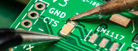
The general surface treatment of PCB includes tin spraying, OSP, immersion gold, etc. The “surface” here refers to the connection points on the PCB that provide electrical connections between electronic components or other systems and the circuits of the PCB, such as pads or contact connections. Bare copper itself has good solderability, but it is easily oxidized and easily contaminated when exposed to air. This is why PCBs must be surface treated.
1.Tin spraying (HASL)
In situations where perforated devices dominate, wave soldering is the best soldering method. The use of hot air leveling (HASL, Hot-air solder leveling) surface treatment technology is sufficient to meet the process requirements of wave soldering. Of course, for situations where the node strength (especially contact connection) is required to be higher, the method of electroplating nickel/gold is often used. HASL is the main surface treatment technology used worldwide, but there are three main driving forces that drive the electronics industry to consider alternative technologies to HASL: cost, new process requirements and lead-free needs.
From a cost point of view, many electronic components such as mobile communications and personal computers are becoming popular consumer products. Only by selling at cost or lower prices can we be invincible in the fierce competition. After the assembly technology developed to SMT, the PCB pads required screen printing and reflow soldering processes during the assembly process. In SMA occasions, the PCB surface treatment process initially still used HASL technology, but with the continuous reduction of SMT devices, the pads and stencil openings also became smaller, and the disadvantages of HASL technology were gradually exposed. The pads treated with HASL technology are not flat enough, and the coplanarity cannot meet the process requirements of fine-pitch pads. Environmental concerns are usually focused on the potential impact of lead on the environment.
2.Organic solderability preservative (OSP)
Organic solderability preservative (OSP, Organic solderability preservative) is an organic coating used to prevent copper from oxidizing before soldering, that is, to protect the solderability of PCB pads from being damaged.
After the PCB surface is treated with OSP, a thin layer of organic compounds is formed on the surface of copper, thereby protecting the copper from oxidation. The thickness of Benzotriazoles OSP is generally 100A°, while the thickness of Imidazoles OSP is thicker, generally 400A°. OSP film is transparent, and it is not easy to distinguish its existence with the naked eye, and it is difficult to detect. During the assembly process (reflow soldering), OSP can easily melt into the solder paste or acidic Flux, while exposing the more active copper surface, and finally forming Sn/Cu intermetallic compounds between the components and the pads. Therefore, OSP has very good properties for treating the welding surface. OSP does not have the problem of lead pollution, so it is environmentally friendly.
Limitations of OSP:
①. Since OSP is transparent and colorless, it is difficult to check and it is difficult to tell whether the PCB has been coated with OSP.
②. OSP itself is insulating and does not conduct electricity.
Benzotriazoles OSP is relatively thin and may not affect electrical testing, but for Imidazoles OSP, the protective film formed is relatively thick, which will affect electrical testing. OSP cannot be used to treat electrical contact surfaces, such as the keyboard surface of keys.
③. OSP needs a stronger Flux during welding, otherwise the protective film cannot be eliminated, resulting in welding defects.
④. During storage, the OSP surface cannot be exposed to acidic substances and the temperature cannot be too high, otherwise the OSP will evaporate.
3.Immersion Gold (ENIG)
Protection mechanism of ENIG:
Ni/Au is plated on the copper surface by chemical methods. The deposition thickness of the inner layer Ni is generally 120~240μin (about 3~6μm), and the deposition thickness of the outer layer Au is relatively thin, generally 2~4μinch (0.05~0.1μm). Ni forms a barrier layer between solder and copper. During welding, the outer Au will quickly melt into the solder, and the solder and Ni will form Ni/Sn intermetallic compounds. The outer gold plating is to prevent Ni oxidation or passivation during storage, so the gold plating layer must be dense enough and the thickness cannot be too thin.
Immersion gold: In this process, the purpose is to deposit a thin and continuous gold protective layer. The thickness of the main gold should not be too thick, otherwise the solder joint will become very brittle, seriously affecting the reliability of welding. Like nickel plating, the working temperature of immersion gold is very high and the time is also very long.
During the immersion process, a replacement reaction will occur-on the surface of nickel, gold replaces nickel, but when the replacement reaches a certain degree, the replacement reaction will automatically stop.
Gold has high strength, abrasion resistance, high temperature resistance, and is not easy to oxidize, so it can prevent nickel oxidation or passivation, and is suitable for working in occasions with high strength requirements.
The surface of the PCB treated with ENIG is very flat and has good coplanarity. It is the best choice for the contact surface of the key. Secondly, ENIG has excellent solderability, and gold will quickly melt into the molten solder, thereby exposing fresh Ni.
Limitations of ENIG:
The process of ENIG is relatively complicated, and if you want to achieve good results, you must strictly control the process parameters. The most troublesome thing is that the surface of the PCB treated with ENIG is prone to black pad effect during ENIG or welding, which has a catastrophic impact on the reliability of the solder joint. The mechanism of black disk generation is very complicated. It occurs at the interface between Ni and gold, which is directly manifested as excessive oxidation of Ni. Too much gold will make the solder joints brittle and affect reliability.
Each surface treatment process has its own unique features and different application ranges. Different surface treatment requirements are required according to the application of different boards. Under the limitation of the manufacturing process, we sometimes make suggestions to customers based on the characteristics of the board, mainly based on the customer’s product application and the company’s process capabilities to make a reasonable choice of surface treatment.


