Build pcb online
Step-by-Step Guide to Designing Your First PCB Online
Designing your first printed circuit board (PCB) online can be an exciting yet daunting task. However, with the right guidance and tools, the process can be streamlined and efficient. This guide aims to provide a comprehensive overview of the steps involved in creating a PCB online, ensuring that even beginners can navigate the process with confidence.
To begin with, it is essential to understand the basic components and functions of a PCB.
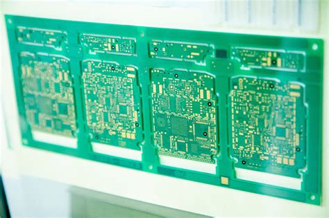
A printed circuit board serves as the foundation for electronic devices, providing both mechanical support and electrical connections for various components. The design process involves creating a layout that optimally places these components and routes electrical connections between them. With this foundational knowledge, you can proceed to select an appropriate online PCB design tool. Numerous platforms are available, each offering unique features and capabilities. Popular options include EasyEDA, KiCad, and Altium Designer. These tools provide user-friendly interfaces and extensive libraries of components, making them suitable for both novices and experienced designers.
Once you have chosen a design tool, the next step is to create a schematic diagram.
This diagram serves as a blueprint for your PCB, detailing the components and their connections. Begin by selecting the necessary components from the tool’s library and placing them on the schematic canvas. It is crucial to ensure that each component is correctly labeled and oriented, as this will affect the subsequent layout process. After placing the components, use the tool’s wiring feature to draw connections between them, following the logical flow of your circuit design.
With the schematic complete, you can transition to the layout phase.
This step involves arranging the components on the PCB and routing the electrical connections, known as traces, between them. Most design tools offer an auto-router feature that can automatically generate these traces based on your schematic. However, manual routing may be necessary for more complex designs or to optimize the layout for performance and manufacturability. During this phase, it is important to consider factors such as trace width, spacing, and layer management to ensure the board’s reliability and functionality.
After finalizing the layout, the next step is to perform a design rule check (DRC).
This automated process verifies that your design adheres to the specified manufacturing constraints and industry standards. The DRC will identify any potential issues, such as overlapping traces or insufficient spacing, allowing you to make necessary adjustments before proceeding. Once the design passes the DRC, you can generate the Gerber files, which are the standard format used by manufacturers to produce PCBs.
The final step involves selecting a PCB manufacturer and submitting your Gerber files for production.
Many online platforms offer integrated manufacturing services, allowing you to seamlessly transition from design to production. When choosing a manufacturer, consider factors such as cost, turnaround time, and quality assurance to ensure that your final product meets your expectations.
In conclusion, designing a PCB online involves a series of methodical steps, from schematic creation to layout and manufacturing. By following this guide and utilizing the available online tools, you can successfully design and produce your first PCB, paving the way for future electronic projects. With practice and experience, you will gain the skills and confidence needed to tackle more complex designs and innovations.

Top Online Tools for PCB Design and Prototyping
In the rapidly evolving world of electronics, the ability to design and prototype printed circuit boards (PCBs) online has become an invaluable asset for engineers, hobbyists, and startups alike. The convenience and accessibility of online tools have revolutionized the way PCBs are developed, allowing for faster iterations and more efficient workflows. As the demand for custom electronics grows, so does the need for reliable and user-friendly online platforms that facilitate PCB design and prototyping. Several top-tier tools have emerged in this space, each offering unique features that cater to different needs and skill levels.
One of the most prominent online tools for PCB design is Autodesk’s Eagle.
Known for its robust feature set and intuitive interface, Eagle provides users with a comprehensive suite of design tools that streamline the PCB creation process. Its schematic editor and layout editor are seamlessly integrated, allowing for real-time updates and error checking. Moreover, Eagle’s extensive component library and community support make it a popular choice among both beginners and seasoned professionals. Transitioning from design to prototyping is made easy with Eagle’s compatibility with various fabrication services, ensuring that users can bring their designs to life with minimal hassle.
Another noteworthy tool is KiCad, an open-source PCB design suite that has gained significant traction in recent years.
KiCad offers a powerful set of features, including a schematic editor, PCB layout editor, and a 3D viewer, all of which are essential for creating complex designs. Its open-source nature means that it is constantly being improved by a dedicated community of developers, ensuring that it remains at the cutting edge of PCB design technology. Furthermore, KiCad’s ability to handle multi-layer boards and its support for various file formats make it a versatile option for those looking to create intricate designs.
For those seeking a more streamlined and user-friendly experience, EasyEDA is an excellent choice.
This web-based tool offers a simplified interface that is perfect for beginners, while still providing advanced features for more experienced users. EasyEDA’s cloud-based platform allows for easy collaboration and sharing of projects, making it ideal for teams working remotely. Additionally, its integration with popular component suppliers like LCSC ensures that users can easily source the parts they need for their designs. The transition from design to production is further facilitated by EasyEDA’s partnership with JLCPCB, one of the leading PCB manufacturers, allowing for seamless ordering and fabrication.
Altium 365 is another powerful tool that deserves mention, particularly for those working in professional environments.
Altium 365 offers a cloud-based platform that enables real-time collaboration and data management, making it an excellent choice for teams working on complex projects. Its advanced design capabilities, coupled with its integration with Altium Designer, provide users with a comprehensive solution for PCB design and prototyping. The platform’s ability to manage design data and facilitate communication between team members ensures that projects are completed efficiently and accurately.
In conclusion, the landscape of online PCB design and prototyping tools is rich with options that cater to a wide range of needs and expertise levels. Whether you are a hobbyist looking to create simple designs or a professional engineer working on complex projects, there is a tool available that can meet your requirements. By leveraging these online platforms, users can streamline their workflows, reduce time to market, and ultimately bring their electronic innovations to life with greater ease and precision.
Benefits of Using Online Platforms for PCB Manufacturing
In recent years, the landscape of printed circuit board (PCB) manufacturing has undergone a significant transformation, largely due to the advent of online platforms. These digital solutions have revolutionized the way engineers and hobbyists alike approach PCB design and production, offering a myriad of benefits that were previously unattainable through traditional methods.
As we delve into the advantages of using online platforms for PCB manufacturing, it becomes evident that these tools not only enhance efficiency but also democratize access to high-quality PCB production.
To begin with, one of the most compelling benefits of online PCB manufacturing platforms is the convenience they offer.
Traditionally, PCB production involved a lengthy process of finding a suitable manufacturer, negotiating terms, and often dealing with geographical constraints. However, online platforms have streamlined this process by providing a centralized hub where users can design, customize, and order PCBs from the comfort of their own homes or offices. This ease of access significantly reduces the time and effort required to bring a PCB design from concept to reality, thereby accelerating project timelines and allowing for more rapid iteration and innovation.
Moreover, online platforms for PCB manufacturing often come equipped with user-friendly design tools that cater to both novices and experienced engineers.
These tools typically feature intuitive interfaces and a range of templates and components, enabling users to create complex designs without the need for extensive technical expertise. As a result, individuals who may have been previously deterred by the technical barriers of PCB design can now participate in the process, fostering a more inclusive environment for innovation and creativity.
In addition to convenience and accessibility, online PCB platforms offer a level of cost-effectiveness that is difficult to match through traditional manufacturing methods.
By leveraging economies of scale and automated processes, these platforms can offer competitive pricing, even for small batch orders. This affordability is particularly beneficial for startups and small businesses that may have limited budgets but still require high-quality PCBs for their products. Furthermore, many online platforms provide instant quotes and transparent pricing structures, allowing users to make informed decisions and manage their budgets more effectively.
Another significant advantage of using online platforms for PCB manufacturing is the ability to access a global network of suppliers and manufacturers.
This connectivity not only broadens the range of options available to users but also fosters a competitive environment that drives innovation and quality improvements. By having access to a diverse pool of manufacturers, users can select partners that best meet their specific needs in terms of quality, turnaround time, and cost. This flexibility is invaluable in a rapidly evolving technological landscape where adaptability is key to success.
Finally, online PCB manufacturing platforms often incorporate advanced features such as real-time design rule checks and automated testing, which help ensure the accuracy and reliability of the final product.
These features minimize the risk of errors and defects, thereby enhancing the overall quality of the PCBs produced. Additionally, many platforms offer comprehensive support and resources, including tutorials, forums, and customer service, to assist users throughout the design and manufacturing process.
In conclusion, the benefits of using online platforms for PCB manufacturing are manifold, encompassing convenience, accessibility, cost-effectiveness, global connectivity, and quality assurance. As these platforms continue to evolve and improve, they are poised to play an increasingly integral role in the future of PCB production, empowering a new generation of innovators and creators to bring their ideas to life with unprecedented ease and efficiency.
Common Mistakes to Avoid When Building PCBs Online
Building printed circuit boards (PCBs) online has become increasingly accessible, thanks to advancements in technology and the proliferation of user-friendly platforms. However, despite the convenience and efficiency these tools offer, there are common mistakes that can hinder the success of your PCB project. Understanding these pitfalls and how to avoid them is crucial for both novice and experienced designers.
One of the most frequent errors is neglecting to thoroughly review the design specifications before submitting them for production.
It is essential to double-check all dimensions, component placements, and routing paths to ensure they align with the intended design. Overlooking these details can lead to costly revisions and delays. To mitigate this risk, it is advisable to use design rule checks (DRC) provided by most PCB design software. These automated checks can identify potential issues such as trace width violations or clearance problems, allowing you to address them before they become significant obstacles.
Another common mistake is underestimating the importance of selecting the right materials and components.
The choice of substrate, copper thickness, and solder mask can significantly impact the performance and durability of the PCB. Additionally, selecting components without considering their availability or lead times can result in unexpected delays. To avoid these issues, it is beneficial to consult with suppliers early in the design process and ensure that all materials and components are readily available and meet the necessary specifications.
Furthermore, inadequate attention to thermal management can lead to overheating and potential failure of the PCB.
It is crucial to incorporate adequate heat dissipation measures, such as thermal vias, heat sinks, or copper pours, especially in high-power applications. Failing to do so can compromise the reliability and longevity of the board. Utilizing simulation tools to model thermal performance can provide valuable insights and help optimize the design for better heat management.
In addition to technical considerations, communication with the PCB manufacturer is often overlooked.
Clear and detailed documentation is vital to ensure that the manufacturer understands your requirements and can produce the board accurately. This includes providing comprehensive fabrication and assembly drawings, as well as specifying any special instructions or tolerances. Establishing a good rapport with the manufacturer and maintaining open lines of communication can prevent misunderstandings and ensure a smoother production process.
Moreover, neglecting to perform a thorough prototype testing phase can lead to unforeseen issues in the final product.
Prototyping allows you to validate the design, identify any functional or performance-related problems, and make necessary adjustments before mass production. Skipping this step can result in significant setbacks and increased costs if defects are discovered later in the process. Therefore, it is prudent to allocate sufficient time and resources for prototyping and testing to ensure the final product meets all requirements.
Lastly, failing to consider the future scalability of the design can limit the potential for upgrades or modifications.
Designing with flexibility in mind, such as incorporating modular components or leaving room for additional features, can facilitate future enhancements and extend the lifespan of the PCB. This forward-thinking approach can save time and resources in the long run, as it reduces the need for complete redesigns when changes are necessary.
In conclusion, while building PCBs online offers numerous advantages, it is essential to be aware of common mistakes that can impede the success of your project. By paying careful attention to design specifications, material selection, thermal management, communication with manufacturers, prototyping, and scalability, you can avoid these pitfalls and ensure a smooth and efficient PCB development process.


