Build Your Own PCB: A Comprehensive Guide for Beginners
Introduction to PCB Design
Printed Circuit Boards (PCBs) form the foundation of nearly all modern electronic devices. From smartphones to microwave ovens, these intricate boards provide the physical platform that connects electronic components in an organized, efficient manner. While commercial electronics typically use professionally manufactured PCBs, hobbyists and engineers increasingly choose to design and fabricate their own boards for prototypes, custom projects, or educational purposes.
Building your own PCB might seem daunting at first, but with the right tools, knowledge, and patience, it’s an achievable and rewarding process. This comprehensive guide will walk you through the entire process from conceptual design to finished product, covering schematic creation, board layout, fabrication methods, and assembly techniques.
Understanding PCB Fundamentals
Before diving into the creation process, it’s essential to understand what a PCB is and how it functions. A PCB is a flat board made of insulating material (typically fiberglass) with conductive copper tracks that electrically connect various components. These boards replace the need for complex wiring by providing predefined pathways for electrical signals.
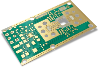
PCB Layers and Composition
Basic PCBs consist of:
- Substrate: The base material (usually FR-4 fiberglass)
- Copper Layer: Thin copper foil laminated to the substrate
- Solder Mask: Protective layer that prevents short circuits
- Silkscreen: Text and symbols for component placement
More complex boards may have multiple copper layers (2, 4, or even 16+ layers) sandwiched between substrate material, allowing for denser component placement and more complex circuits.
Common PCB Components
Understanding common components will help in designing your board:
- Resistors: Limit current flow
- Capacitors: Store and release electrical energy
- Inductors: Store energy in a magnetic field
- Diodes: Allow current flow in one direction
- Transistors: Amplify or switch electronic signals
- Integrated Circuits (ICs): Complex circuits in small packages
Step 1: Circuit Design and Schematic Creation
The first step in building your PCB is designing the circuit you want to implement. This begins with creating a schematic diagram—a symbolic representation of your electronic circuit.
Choosing Schematic Software
Several software options are available for schematic capture:
- KiCad: Free, open-source, and powerful
- Eagle: Popular with hobbyists (now free for basic use)
- Altium Designer: Professional-grade (expensive)
- Fritzing: Beginner-friendly but limited
- EasyEDA: Web-based option with integration to manufacturing services
For beginners, KiCad offers an excellent balance of capability and accessibility without cost barriers.
Drawing Your Schematic
When creating your schematic:
- Place all required components from the library
- Connect components with wires (nets)
- Label important connections
- Verify all connections are correct
- Run Electrical Rules Check (ERC) to catch errors
Ensure each component has a proper value (resistance, capacitance, etc.) and unique reference designator (R1, C2, Q3, etc.).
Step 2: PCB Layout Design
After completing your schematic, you’ll translate it into a physical board layout. This process involves arranging components and routing copper traces between them.
Board Setup Considerations
- Board Dimensions: Determine the size based on component placement and enclosure requirements
- Layer Count: Start with single or double-layer for simplicity
- Design Rules: Set minimum trace widths, clearances, and via sizes
- Grid System: Use a grid (typically 0.05″ or 1.27mm) for component placement
Component Placement Strategies
Effective component placement is crucial:
- Group related components together
- Place connectors near board edges
- Consider heat dissipation for power components
- Orient components for easiest routing
- Leave space for debugging/probing
Routing Techniques
Routing connects components according to your schematic:
- Power Traces: Make these wider (10-50mil) to handle current
- Signal Traces: Can be narrower (6-10mil) for low-current signals
- Ground Planes: Use copper pours for better grounding
- Avoid 90° Angles: Use 45° angles to reduce EMI
- Via Usage: Connect between layers when necessary
Design Rule Check (DRC)
Always run DRC before finalizing your design to catch:
- Trace spacing violations
- Unrouted nets
- Incorrect hole sizes
- Other manufacturing issues
Step 3: PCB Fabrication Methods
With your design complete, you have several options for physical fabrication:
Professional PCB Manufacturing
Services like:
- JLCPCB
- PCBWay
- OSH Park
- Seeed Studio
Offer high-quality, low-cost boards (often $5-20 for small quantities) with:
- Professional solder mask and silkscreen
- Precise drilling and plating
- Multiple layer options
- Typically 1-2 week turnaround
DIY Fabrication Methods
For immediate results or educational purposes, consider these DIY methods:
1. Toner Transfer Method
- Print mirrored design on glossy paper using laser printer
- Iron onto cleaned copper clad board
- Soak in water to remove paper
- Etch away exposed copper
2. Photoresist Method
- Apply photosensitive coating to copper board
- Expose to UV light through printed transparency
- Develop to remove unexposed resist
- Etch remaining copper
3. CNC Milling
- Use a desktop CNC machine to mechanically remove unwanted copper
- No chemicals required
- Limited resolution compared to etching
4. Direct Ink Printing
- Special conductive ink printers
- Limited to simple circuits
- No etching required
Etching Process
For chemical etching:
- Use ferric chloride or ammonium persulfate as etchant
- Etch until all unwanted copper dissolves
- Neutralize and properly dispose of chemicals
- Remove resist with acetone or sandpaper
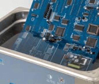
Step 4: Drilling and Finishing
After etching:
- Drill Holes: Use a small drill press or hand tool (typically 0.8-1.0mm for most components)
- Clean Board: Remove any remaining resist or oxidation
- Apply Finish (optional):
- Tin plating (solder or chemical)
- Conformal coating for protection
- Solder mask (UV-curable DIY options available)
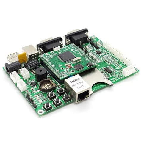
Step 5: Component Assembly
With your fabricated board ready, it’s time to populate it with components.
Soldering Techniques
- Through-Hole Components:
- Insert leads through holes
- Bend slightly to hold in place
- Solder from opposite side
- Trim excess leads
- Surface Mount (SMD) Components:
- Apply solder paste to pads (stencil or syringe)
- Place components with tweezers
- Reflow with hot air or skillet
- Alternatively, hand-solder with fine tip iron
Soldering Tips
- Use appropriate temperature (300-350°C for leaded solder)
- Keep iron tip clean and tinned
- Apply heat to both pad and component lead
- Feed solder to the joint, not the iron
- Avoid excessive heat to prevent pad lifting
Inspection and Rework
After soldering:
- Visually inspect for:
- Cold solder joints (dull, grainy appearance)
- Bridges between pins
- Tombstoning (SMD components standing up)
- Use multimeter to check:
- Continuity where expected
- No shorts between power rails
- Perform necessary rework:
- Add solder to insufficient joints
- Remove bridges with solder wick
- Replace faulty components
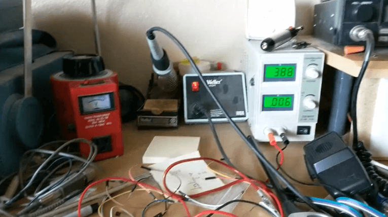
Step 6: Testing and Debugging
Before applying power:
- Verify correct power supply polarity and voltage
- Check for shorts between power and ground
- Use a current-limited power supply if possible
Debugging techniques:
- Visual Inspection: Look for physical defects
- Power Analysis: Measure current draw
- Signal Tracing: Follow signals with oscilloscope
- Divide and Conquer: Test subsections independently
- Thermal Imaging: Identify hot spots (if available)
Advanced Techniques
As you gain experience, consider these advanced methods:
Multilayer Boards
- Route complex designs by adding internal layers
- Requires careful planning of layer stackup
- Professional fabrication recommended
High-Speed Design
- Impedance-controlled traces
- Length matching for differential pairs
- Proper grounding techniques
Flexible PCBs
- Use polyimide substrate
- Allows for bending and unique form factors
Resources and Continuing Education
To further develop your PCB skills:
Learning Resources
- Books:
- “PCB Design for Real-World EMI Control” by Bruce Archambeault
- “High-Speed Digital Design” by Howard Johnson
- Online Courses:
- Udemy PCB design courses
- Coursera electronics offerings
- YouTube Channels:
- EEVblog
- GreatScott!
- Contextual Electronics
Community Support
- Forums:
- EEVblog forum
- Reddit r/PrintedCircuitBoard
- Open-Source Projects:
- GitHub electronics projects
- Hackaday.io
Conclusion
Building your own PCBs is an incredibly rewarding skill that bridges the gap between theoretical electronics and practical implementation. While the process involves multiple steps—from schematic design to physical fabrication and assembly—each stage becomes more manageable with practice. Modern tools and affordable manufacturing services have democratized PCB production, making it accessible to hobbyists, students, and professionals alike.
Starting with simple single-layer designs and gradually progressing to more complex boards allows for skill development without frustration. Remember that even experienced engineers make mistakes—debugging is an integral part of the process. Each completed project will enhance your understanding of electronics and PCB design principles.
Whether you’re creating prototypes, custom devices, or simply exploring electronics as a hobby, the ability to design and build your own PCBs opens up a world of possibilities. With the foundational knowledge provided in this guide and continued practice, you’ll be well on your way to mastering this essential engineering skill.