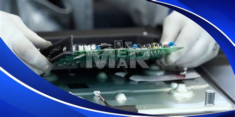
Building circuit boards
PCB design is the entire process of creating a printed circuit board (PCB) through collaboration and integration between multiple disciplines and domains, including electrical, mechanical, software, systems, test, and manufacturing. It is a team effort that requires constant two-way communication.
Success in PCB design now also includes achieving supply chain resiliency for electronic system design. This includes implementing an outside-in approach with supply chain intelligence by shifting left the most well-known parts availability, BOM verification, and alternatives verification at the design point. Having knowledge, wisdom, and optimization in design are the keys to achieving resilient design success in PCB design.
The state of designing electronic products today is more complex and tighter than ever before. Design teams must deliver more complex products within tighter schedules, but they waste valuable time on non-productive tasks. Connect them through all engineering disciplines and provide them with best-in-class solutions to thrive through a collaborative approach to electronic system design.
GET PCB MANUFACTURING AND ASSEMBLY QUOTE NOW!
PCB Design: Cityscape
One of the simplest explanations or metaphors for PCB design that I really like is that it is like “designing a city.” A city, the land (real estate), structural foundation, buildings, houses, and roads are all connected to each other.
The land (real estate) and structural foundation of a city represent the stacking of PCBs. The buildings and houses represent the electrical and mechanical components placed on the PCB, and the roads represent the copper wires and vias that connect everything as needed.
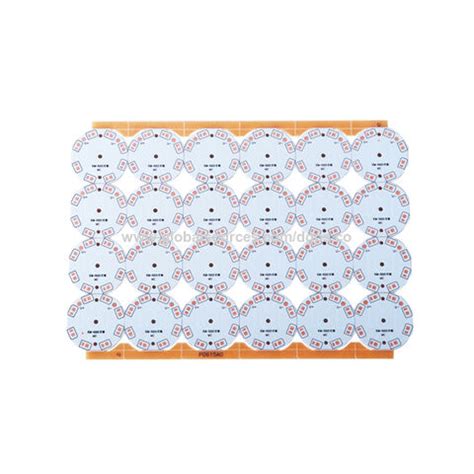
The bare PCB consists of a pattern of pads used to connect/solder the components to the PCB. They are interconnected by conductive printed lines called traces on a non-conductive substrate. They provide the pathways for the circuit to function.
This is commonly referred to as a printed wiring board (PWB). It is important to note that until all the necessary components are soldered to the PWB, it is not considered an assembly. Once soldered to the PWB, the circuit is complete. A fully assembled/populated PCB produces a fully functional ecosystem, which is a metaphorical comparison between PCB design and a design city.
Once the PCB is fully populated with all the necessary components, at this stage or assembly level, it is often referred to as a printed circuit assembly (PCA), printed circuit board assembly (PWBA), or circuit card assembly, depending on how you choose to refer to the fully populated printed circuit board.
The Role of the PCB Designer
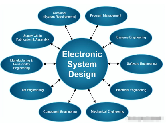
Figure 1 – Project Stakeholders (Departments)
Like many engineering disciplines related to PCB design (electronic system design), the PCB designer (printed circuit layout professional) plays a critical role that is typically located in the electrical engineering department.
See Figure 1 for the key stakeholders (departments) who typically collaborate throughout the design process to achieve the project end goal, whether it is an internal company goal/milestone, or an external customer requirement.
With such a diverse set of key stakeholders, both internal and external, organized complexity requires multidisciplinary collaboration and integration. See Figure 2 for an example of today’s system-level connectivity – Organizational Complexity.
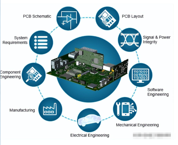
Figure 2 – System-Level Connectivity – Organized Complexity Requires Multidisciplinary Collaboration
With such a diverse set of key stakeholders, both internal and external, organized complexity requires multidisciplinary collaboration and integration.
See Figure 2 for an example of today’s system-level connectivity – Organizational Complexity.
Typically, PCB design falls into the hardware (HW) design category of engineering. It ties in with the electrical, mechanical, software, system, test, and manufacturing disciplines, including electrical (ECAD) and mechanical (MCAD) designers.
PCB design requires a lot of input and detail from multiple disciplines and their respective areas to help define, validate, and produce the final product. An example of these is as follows:
System-level requirements/architecture definition
Mechanical, electrical, software, system, and test requirements/constraints
Signal integrity (SI) / electromagnetic compatibility (EMC), power integrity (PI) / thermal analysis
Design for manufacturing (DFM) and producibility guidelines
Supply chain resiliency regarding component sourcing
Hardware is typically created from mechanical definitions and constraints that are fed into the PCB layout along with electrical input/requirements, including schematics (graphic symbols and diagrams that describe electronic circuits) and electrical and physical constraints that meet the final product definition/requirements.
PCB design has evolved from early sticky back component patterns and tape to polyester film sheets that are then photographed to create production tooling masters for manufacturing.
As PCB design has evolved over the decades, the processes and individual roles of key stakeholders (who does what and when in the design process) have also changed.
Schematics are created by electrical or electronics engineers. Mechanical engineers provide the physical package or envelope with all the physical requirements and constraints.
This mechanical information feeds into the PCB layout. The layout specialist (electrical designer) then designs the PCB layout, which is a result of multidisciplinary collaboration. This specialist has been serving as the hub or focal point for the project team to gather all the inputs/requirements that need to be implemented into the PCB design.
Printed Circuit Engineering: Definition
The knowledge, skill sets, and experience required to be successful in PCB design has evolved into what is known today as printed circuit engineering. This evolution requires a comprehensive understanding of design for package solubility, performance, and manufacturing. The printed circuit layout professional/specialty in today’s industry now cross-pollinates the necessary skill sets between the electrical, mechanical, software, test, and manufacturing disciplines. You can now understand why it is safe to say that the PCB design process has evolved from an isolated/individual effort to a multidisciplinary, multi-domain team effort and a specialty in its own right for printed circuit layout.
To help guide individuals entering or continuing in the industry, in 2017 the IPC Technical Activities Executive Committee (TAEC) accepted a recommended definition for the printed circuit engineering layout professional to be incorporated into the IPC-2200 series of standards. It is important to note that the printed circuit engineering layout professional is only one of the important roles in the grand scheme of PCB design. It does not cover all roles in PCB design. The generally accepted recommended definitions are shown below and graphically.
GET PCB AND ASSEMBLY SERVICE QUOTE NOW!
IPC-22XX 1.X. Definition of the Printed Circuit Engineering Layout Profession
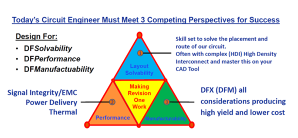
Figure 3 – Design Engineering Triangle – 3 Perspectives of Success
The following overview describes the core knowledge and capabilities to best perform the Printed Circuit Engineering Layout role as an independent professional or as an engineer performing this role. Today’s designer must address 3 perspectives of success with the goal of getting the first iteration to work as expected.
Layout Solvability – Complex Packaging Skill Set
Performance – Signal, PWR and Thermal Performance at All Layers
Manufacturability – DFX Considerations for High Yield and Low Cost
The results provide the maximum achievable component placement/routing density, optimal electrical performance, and efficient, high yield and defect-free manufacturing.
PCB Design Best Practices
Involving all required stakeholders at the initial stages of the PCB design process and by implementing industry PCB design best practices is key to overall success.
Multidisciplinary and multi-domain collaboration and integration and continuous two-way communication between all stakeholders is essential to breaking down barriers and working in silos. The 5 pillars of industry PCB design best practices are highly recommended to achieve PCB design success. These 5 pillars are as follows:
Digital Integration and Optimization
Engineering Productivity and Efficiency
Digital Prototype Driven Verification
System-Level Model-Based Engineering
Supply Chain Resilience
PCB Design Has Evolved
Reflecting on the original question: “What is PCB Design?”, it can be seen why there is so much that encompasses PCB design and why it requires more than a simple definition. PCB design has evolved into the printed circuit engineering of electronic system design. In short, PCB design has become a multidisciplinary, multi-domain process that requires collaboration/integration and digital transformation.