Calculation of Parasitic Capacitance and Inductance in PCB Design
Abstract
This paper provides a comprehensive analysis of parasitic capacitance and inductance in printed circuit board (PCB) designs. As modern electronics continue to operate at higher frequencies and with greater signal integrity requirements, understanding and calculating these parasitic elements becomes crucial for successful circuit implementation. The article presents theoretical foundations, calculation methods, and practical considerations for estimating parasitic capacitance and inductance in various PCB structures including traces, vias, and component pads. Both analytical approaches and empirical techniques are discussed, along with mitigation strategies to minimize parasitic effects in high-speed designs.
1. Introduction
In the realm of high-frequency PCB design, parasitic capacitance and inductance emerge as critical factors affecting circuit performance. These unintended circuit elements, inherent in all physical implementations of electronic circuits, can significantly alter signal behavior, leading to issues such as signal degradation, crosstalk, power integrity problems, and electromagnetic interference (EMI).
Parasitic elements become particularly problematic as signal rise times decrease and operating frequencies increase. Modern digital systems with clock frequencies in the gigahertz range and analog RF circuits operating at microwave frequencies demand precise control over these parasitic effects. This paper focuses on the calculation methods that allow designers to predict and account for parasitic capacitance and inductance during the design phase.
2. Fundamentals of Parasitic Elements
2.1 Parasitic Capacitance
Parasitic capacitance refers to the unintended capacitance that exists between conductors separated by an insulating material (dielectric). In PCBs, this occurs between:
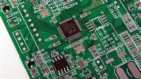
- Adjacent signal traces
- Traces and reference planes
- Component leads and pads
- Parallel vias in high-density designs
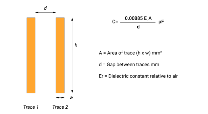
The general formula for capacitance between two parallel conductors is:
C = ε₀εᵣ(A/d)
Where:
- C = capacitance (Farads)
- ε₀ = permittivity of free space (8.854×10⁻¹² F/m)
- εᵣ = relative permittivity of the dielectric material
- A = overlapping area of conductors (m²)
- d = separation distance between conductors (m)
2.2 Parasitic Inductance
Parasitic inductance refers to the unintended inductance associated with current-carrying conductors. In PCBs, this manifests in:
- Trace inductance
- Via inductance
- Bond wire inductance in components
- Loop inductance in power distribution networks
The general formula for the inductance of a straight conductor is more complex and depends on the geometry. For a straight round wire, the partial self-inductance is given by:
L = (μ₀μᵣl/2π) [ln(2l/r) – 3/4]
Where:
- L = inductance (Henries)
- μ₀ = permeability of free space (4π×10⁻⁷ H/m)
- μᵣ = relative permeability of the material (~1 for most PCB materials)
- l = length of conductor (m)
- r = radius of conductor (m)
3. Calculation Methods for PCB Structures
3.1 Microstrip Transmission Lines
Microstrips (surface traces over a reference plane) are common in PCB designs. The parasitic capacitance per unit length (C’) and inductance per unit length (L’) can be calculated using:
C’ = ε₀εᵣ_eff(w/h + 2.42 – 0.44h/w + (1 – h/w)⁶)
L’ = μ₀μᵣ(h/w + 1.393 + 0.667ln(w/h + 1.444))
Where:
- w = trace width
- h = height above reference plane
- εᵣ_eff = effective dielectric constant, given by:
εᵣ_eff = (εᵣ + 1)/2 + (εᵣ – 1)/2(1 + 12h/w)⁻¹/²
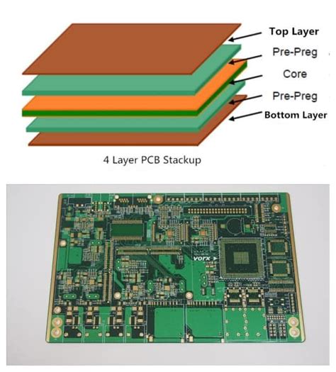
3.2 Stripline Transmission Lines
For embedded traces between two reference planes (striplines), the calculations differ:
C’ = 2ε₀εᵣw/(b – t) + C_fringe
L’ = μ₀μᵣ(b – t)/w
Where:
- b = spacing between reference planes
- t = trace thickness
- C_fringe accounts for fringing fields and can be approximated as 0.07 pF/cm for typical PCB dimensions
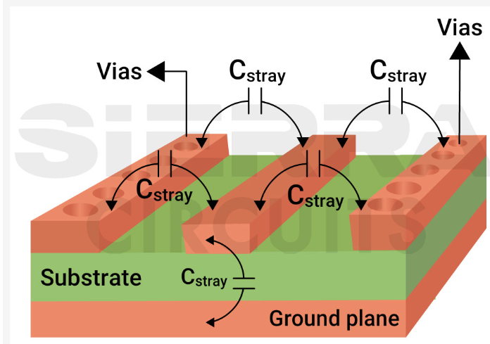
3.3 Via Parasitics
Vias contribute both capacitance and inductance to the signal path. The approximate via capacitance is:
C_via = (1.41ε₀εᵣTD₁)/(D₂ – D₁)
Where:
- T = board thickness
- D₁ = via pad diameter
- D₂ = clearance hole diameter in ground plane
The via inductance is approximately:
L_via = μ₀h[ln(4h/d) + 1]
Where:
- h = via length (board thickness)
- d = via diameter
3.4 Parallel Traces (Crosstalk)
For two parallel traces of length l separated by distance s, running at height h above a reference plane, the mutual capacitance Cₘ and mutual inductance Lₘ can be approximated as:
Cₘ ≈ (πε₀εᵣl)/cosh⁻¹(s/h)
Lₘ ≈ (μ₀l/π)cosh⁻¹(s/h)
4. Advanced Calculation Techniques
4.1 Numerical Methods
For complex geometries, numerical methods such as finite element analysis (FEA) or method of moments (MoM) provide more accurate results. Popular tools include:
- 2D field solvers for cross-sectional analysis
- 3D full-wave electromagnetic simulators
- Partial element equivalent circuit (PEEC) methods
4.2 Empirical Formulas
Many empirical formulas have been developed through curve fitting to measurement data. For example, the modified Wheeler formula for spiral inductor inductance:
L = K₁μ₀n²d_avg/[1 + K₂ρ]
Where:
- K₁, K₂ = geometry-dependent constants
- n = number of turns
- d_avg = average diameter
- ρ = fill ratio
4.3 Measurement-Based Extraction
Time-domain reflectometry (TDR) and vector network analyzer (VNA) measurements can be used to extract parasitic elements from physical prototypes.
5. Practical Considerations and Mitigation Strategies
5.1 Reducing Parasitic Capacitance
- Increase spacing between conductors
- Use lower dielectric constant materials
- Minimize parallel run lengths
- Implement guard traces or ground shields
- Reduce pad sizes for components
5.2 Reducing Parasitic Inductance
- Use wider traces for high-current paths
- Minimize loop areas in current return paths
- Employ multiple vias in parallel
- Place decoupling capacitors close to IC power pins
- Use power and ground planes instead of traces
5.3 Frequency-Dependent Effects
At high frequencies, additional considerations arise:
- Skin effect increases effective resistance
- Dielectric losses become significant
- Proximity effects alter current distribution
6. Conclusion
Accurate calculation of parasitic capacitance and inductance is essential for successful high-speed PCB design. While analytical formulas provide reasonable estimates for simple geometries, complex designs often require numerical simulation or empirical approaches. Designers must balance the need for precise calculations with practical design constraints, always considering that all physical implementations involve trade-offs between various parasitic effects.
As operating frequencies continue to rise, the importance of proper parasitic management grows correspondingly. Future developments in PCB materials and manufacturing techniques may alter some of the specific calculation methods, but the fundamental principles discussed in this paper will remain relevant for understanding and controlling parasitic effects in electronic circuits.