Camera PCB Layout and Routing Design Considerations
Introduction
In today’s increasingly visual world, camera systems have become ubiquitous across countless applications – from smartphones and security systems to automotive applications and industrial machine vision. The performance of these camera systems heavily depends on the quality of their printed circuit board (PCB) design. Proper PCB layout and routing for camera modules requires careful consideration of signal integrity, power distribution, electromagnetic interference (EMI), and thermal management.
This article provides a comprehensive guide to camera PCB design, covering critical aspects that engineers must address to ensure optimal image quality, reliable operation, and robust performance. We’ll examine key considerations for both the analog and digital portions of camera designs, with particular focus on high-speed interfaces like MIPI CSI-2.
1. System Partitioning and Component Placement
1.1 Functional Block Partitioning
Effective camera PCB design begins with proper system partitioning:
- Sensor and analog front-end: This includes the image sensor itself and supporting components like voltage regulators, clock circuits, and analog signal conditioning.
- Digital processing: Typically includes the image signal processor (ISP), memory, and associated digital logic.
- Interface circuitry: Components handling the camera’s communication with the host system (MIPI, USB, LVDS, etc.).
- Power delivery network: Voltage regulators, filtering, and power distribution across the board.
1.2 Placement Guidelines
- Place the image sensor at the center of the layout to minimize trace lengths to all supporting components
- Position voltage regulators close to their loads but away from sensitive analog circuits
- Keep high-speed digital components away from analog sections
- Place decoupling capacitors as close as possible to power pins
- Consider thermal management in component placement – allow for heat dissipation from high-power components
2. Power Distribution Design
2.1 Power Plane Strategy
- Use separate power planes for different voltage domains (sensor analog, sensor digital, ISP, etc.)
- Implement split planes or moats between noisy digital supplies and sensitive analog supplies
- Maintain continuous ground plane beneath all power planes for proper return paths
2.2 Decoupling and Filtering
- Use a combination of bulk, ceramic, and high-frequency capacitors
- Typical values: 10µF bulk, 0.1µF ceramic, and 1nF high-frequency near power pins
- Implement π-filters for sensitive analog supplies (e.g., sensor analog power)
- Place ferrite beads between digital and analog power domains when needed
2.3 Grounding Considerations
- Use a single, solid ground plane whenever possible
- If split grounds are necessary, connect at a single point near the power supply
- Ensure low-impedance ground connections for all components
- Pay special attention to ground connections for the image sensor
3. Signal Integrity for High-Speed Interfaces
Modern camera systems typically use high-speed serial interfaces like MIPI CSI-2, with data rates often exceeding 1Gbps per lane. Proper routing is critical for these signals.
3.1 MIPI CSI-2 Routing Guidelines
- Maintain 100Ω differential impedance for D-PHY pairs
- Keep lane-to-lane skew <100ps (typically <5mm length mismatch)
- Match lengths within differential pairs to <10mil mismatch
- Route all data lanes and clock with similar lengths (±5% tolerance)
- Avoid vias when possible – if necessary, use symmetrical via structures
3.2 General High-Speed Routing Practices
- Avoid 90° bends – use 45° angles or curved traces
- Maintain consistent trace width along the entire route
- Provide adequate spacing between differential pairs (≥3× trace width)
- Keep high-speed traces away from board edges and noisy components
- Minimize parallel runs of high-speed signals to reduce crosstalk
4. Analog Signal Considerations
4.1 Sensor Analog Routing
- Keep analog traces as short as possible
- Use guard rings or ground shields for critical analog signals
- Avoid routing analog traces near or parallel to digital signals
- Implement proper termination for analog lines as specified by sensor manufacturer
4.2 Clock Distribution
- Route clock signals first, with the shortest possible paths
- Use ground guards for clock traces
- Avoid routing clocks near sensitive analog circuits
- Consider using low-jitter clock generators for high-performance applications
5. EMI/EMC Considerations
5.1 Radiated Emissions Control
- Implement proper grounding and shielding strategies
- Use stitching vias along board edges to contain high-frequency energy
- Consider shielded connectors or board-level shielding for critical sections
- Use spread-spectrum clocking where possible and appropriate
5.2 Susceptibility Protection
- Implement proper filtering on all I/O lines
- Use TVS diodes for ESD protection on external interfaces
- Consider common-mode chokes on differential pairs entering/leaving the board
6. Thermal Management
6.1 Heat Dissipation Techniques
- Use thermal vias under high-power components (image sensors, ISPs)
- Consider copper pours or thermal pads for heat spreading
- Ensure adequate airflow in the final product enclosure
- For high-power designs, consider thermal interface materials or heatsinks
6.2 Thermal-Induced Performance Issues
- Be aware of sensor performance changes with temperature
- Account for thermal expansion in mechanical designs
- Monitor temperature-dependent parameters like dark current in image sensors
7. Manufacturing Considerations
7.1 DFM Guidelines
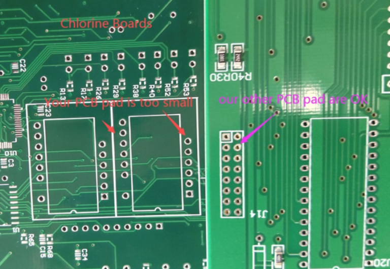
- Follow manufacturer’s recommended pad layouts for image sensors
- Ensure proper solder mask definitions for fine-pitch components
- Consider stencil design for proper solder paste deposition
- Account for PCB warpage during reflow, especially for large boards
7.2 Testability
- Include test points for critical signals and power rails
- Consider boundary scan or other test access mechanisms
- Provide adequate space for probe access if needed
8. Special Considerations for Different Camera Types
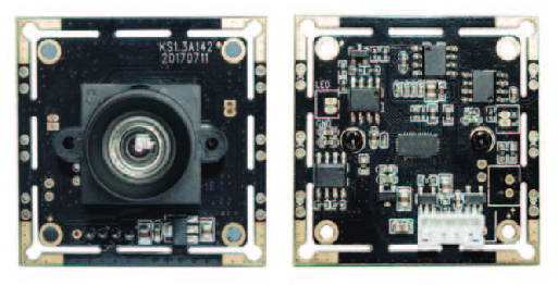
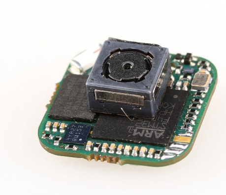
8.1 Smartphone Cameras
- Extreme space constraints require careful layer stackup planning
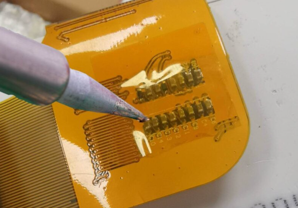
- Flex PCB interconnects require special attention to mechanical reliability
- Very high-density component placement demands meticulous power distribution
8.2 Automotive Cameras
- Must meet stringent automotive reliability standards
- Wide temperature range operation requires robust thermal design
- Vibration resistance impacts component selection and mechanical design
8.3 Industrial/Machine Vision
- Often require higher power for illumination systems
- May need to support multiple camera synchronization
- Frequently require ruggedized designs for harsh environments
9. Layer Stackup Recommendations
A typical camera PCB stackup might include:
- Top Layer: Components and critical signal routing
- Ground Plane: Solid return path
- Power Plane(s): Split as needed for multiple voltages
- Signal Layer: Additional routing
- Ground Plane: Additional return paths
- Bottom Layer: Components and less critical routing
For high-density designs, more layers may be necessary. Always consult with your PCB manufacturer for optimal stackup based on your specific requirements.
10. Verification and Testing
10.1 Pre-Layout Verification
- Perform signal integrity simulations for critical high-speed interfaces
- Model power distribution network to verify voltage drop and decoupling
- Check for potential EMI issues through simulation
10.2 Post-Layout Verification
- Perform design rule checks (DRC) for manufacturing constraints
- Run electrical rule checks (ERC) for connectivity verification
- Verify impedance calculations for critical traces
- Check for timing violations in high-speed interfaces
10.3 Prototype Testing
- Measure power supply noise and ripple
- Validate signal integrity with oscilloscope or TDR measurements
- Test for EMI compliance
- Perform image quality testing under various operating conditions
Conclusion
Designing camera PCBs requires careful attention to numerous factors that can significantly impact performance. From proper power distribution to meticulous high-speed routing, each aspect of the design must be carefully considered to achieve optimal image quality and reliable operation. By following the guidelines outlined in this article—proper partitioning, careful component placement, robust power delivery, controlled impedance routing, and thorough verification—engineers can create camera PCB designs that meet the demanding requirements of modern imaging applications.
As camera technology continues to evolve with higher resolutions, faster frame rates, and more compact form factors, PCB design challenges will only increase. Staying current with the latest design techniques and manufacturing capabilities will be essential for creating successful camera designs in this rapidly advancing field.