Causes and effects of EMI in PCB
There are many reasons for EMI in PCB, such as RF current, common mode level, ground loop, impedance mismatch, magnetic flux, etc. In order to master EMI, we need to gradually understand these causes and their effects. Although we can learn the mathematical basis of EMI phenomenon directly from electromagnetic theory, it is a very hard and long road. For general engineers, simple and clear descriptions are more important. This article will explore the “source of electricity” on PCB, the application of Maxwell’s equations, and the concept of minimizing magnetic flux.
Source of electricity
In contrast to the source of magnetism, the source of electricity is modeled as a time-varying electric dipole. This means that there are two separate, oppositely polarized, time-varying point charges adjacent to each other. The two ends of the dipole contain changes in charge. This change in charge is caused by the continuous flow of current throughout the length of the dipole. Using the oscillator output signal to drive an unterminated antenna, this circuit can be used to represent the source of electricity. However, this circuit cannot be explained using low-frequency circuit principles. Regardless of the finite propagation speed of the signal in this circuit (which is determined by the dielectric constant of the non-magnetic material), radio frequency currents will be generated in this circuit anyway. This is because the propagation speed is finite, not infinite. The assumption is that the wire contains the same voltage at all points and that the circuit is instantly balanced at any point. The electromagnetic field generated by this electrical source is a function of four variables:
- The amplitude of the current in the loop: the electromagnetic field is proportional to the amount of current flowing in the dipole.
- The relationship between the polarity of the dipole and the measuring device: As with the magnetic source, the polarity of the dipole must be the same as the polarity of the antenna of the measuring device.
- The size of the dipole: the electromagnetic field is proportional to the length of the current component, but the length of the trace must be only a fraction of the wavelength. The larger the dipole, the lower the frequency measured at the antenna. For a certain size, the antenna will resonate at a certain frequency.
- Distance: the electric and magnetic fields are related to each other. The strength of both is proportional to the distance. In the far field, its behavior is similar to the loop source (magnetic source), and an electromagnetic plane wave will appear. When approaching the “point source”, the dependence of the electric and magnetic fields on the distance increases.
The relationship between the near field (magnetic and electric components) and the far field is shown in Figure 1. All waves are a combination of magnetic and electric field components. This combination is called the “Poynting vector”. In fact, there is no single electric or magnetic wave. The reason why we can measure plane waves is that for a small antenna, its wavefront looks like a plane at a distance of several wavelengths from the source.
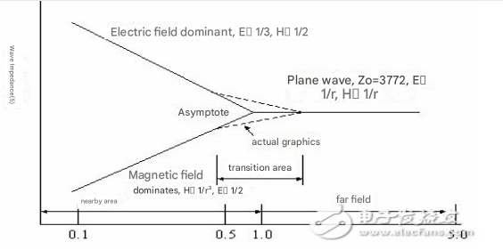
Figure 1: Relationship between wave impedance and distance
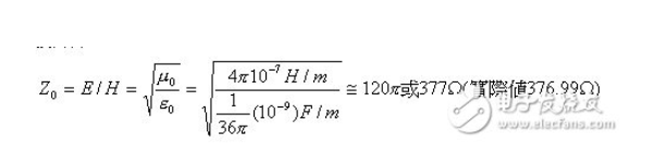
This appearance is the physical “contour” observed by the antenna; it is like skipping from the river bank to the river, and the water waves we see are ripples. Field propagation is radiating outward from the point source of the field at the speed of light; among them,. The electric field component is measured in V/m and the magnetic field component is measured in A/m. The ratio of the electric field (E) to the magnetic field (H) is the impedance of free space. It must be emphasized here that in plane waves, the wave impedance Z0, or the characteristic impedance of free space, is independent of distance and the characteristics of the point source. For a plane wave in free space:
The energy carried by the wavefront is measured in watts/m2.
For most applications of Maxwell’s equations, the noise coupling method can represent the model of equivalent components. For example: a time-varying electric field between two conductors can represent a capacitor. Between the same two conductors, a time-varying magnetic field can represent mutual inductance. Figure 2 shows these two noise coupling mechanisms.
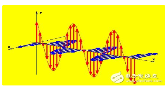
Figure 2: Noise coupling mechanism
The shape of a plane wave
For this noise coupling method to be correct, the actual size of the circuit must be smaller than the wavelength of the signal. If this model is not really correct, it is still possible to use lumped components to illustrate EMC for the following reasons:
- Maxwell’s equations cannot be directly applied in most real-world situations due to complex boundary conditions. If we are not confident in the approximation of the lumped model, then the model is incorrect. However, most lumped components (or discrete components) are reliable.
- Numerical models do not show how noise is generated based on system parameters. Even if there is a model that may be the answer, the parameters related to the system cannot be predicted, identified, and displayed. Among all the available models, the model established by lumped components is the best.
Why is this theory and discussion of Maxwell’s equations important for PCB design and layout? The answer is simple. We must first know how electromagnetic fields are generated, and then we can reduce the electromagnetic fields generated by RF in the PCB. This is related to reducing the RF current in the circuit. This RF current is directly related to the signal distribution network, bypassing and coupling. The RF current will eventually form harmonics of the frequency and other digital signals. The signal distribution network must be as small as possible so that the loop area of the RF return current can be minimized. Bypassing and coupling are related to the maximum current and must be generated through the power distribution network; and the power distribution network, by definition, has a large loop area for the RF return current.
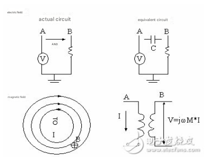
Figure 3: Noise coupling method
Application of Maxwell equations
So far, the basic concept of Maxwell equations has been introduced. But how to relate this knowledge of physics and advanced calculus to EMC in PCB? In order to fully understand it, Maxwell equations must be simplified before it can be applied to PCB layout. To apply it, we can relate Maxwell equations to Ohm’s law:
Ohm’s law (time domain): V = I * R
Ohm’s law (frequency domain): Vrf= “Irf” * Z
V is voltage, I is current, R is resistance, Z is impedance (R + jX), and rf refers to RF energy. If RF current exists in a PCB trace and the trace has a fixed impedance value, an RF voltage will be generated and is proportional to the RF current. Note that in the electromagnetic wave model, R is replaced by Z, which is a complex number with resistance (real number) and reactance (imaginary number).
There are many forms of impedance equations, depending on whether we want to examine the impedance of plane waves, circuit impedance, etc. For wires or PCB traces, the following formula can be used:
Causes and effects of EMI in PCB
Wherein, XL=2πfL is the only component related to wires or PCB traces in this formula.
Xc=1/2(2πfC), ω=2πf
When both the resistance and inductance of a component are known, such as a ferrite bead-on-lead, a resistor, a capacitor, or other device with parasitic components, the impedance must be considered to be affected by frequency. The following formula can be applied:
When the frequency is greater than a few kHz, the reactance value is usually larger than R; but in some cases, this does not happen. Current will choose the path with the least impedance. Below a few kHz, the path with the least impedance is the resistor; above a few kHz, the path with the least reactance becomes dominant. At this point, because most circuits operate at frequencies above a few kHz, the idea that “current will choose the path with the least impedance” becomes incorrect because it cannot correctly explain “how current flows in a transmission line.”
For a wire carrying current at a frequency above 10 kHz, because its current always chooses the path with the least impedance, its impedance is equivalent to the path with the least reactance. If the load impedance connected to the wire, cable, or trace is larger than the capacitance in parallel with it in the transmission line path, then inductance will become dominant. If all connected wires have approximately the same cross-sectional area, the path with the least inductance is the path with the smallest loop area. The smaller the loop area, the smaller the inductance, so the current will flow in this path.
Every trace has a finite impedance value. “Trace inductance” is the only reason why RF energy can be generated in a PCB. It can even be caused by long solder wires connecting the silicon chip to the mounting pad. Winding wires on the board will produce high inductance values, especially when the traces are long. Long traces are those with long winding lengths, which will cause the signal that propagates back and forth in the trace to be delayed before the next trigger signal is generated (this is observed in the time domain) before it returns to the source driver. In the frequency domain, it refers to a long transmission line (trace) whose total length is approximately greater than λ/10 of the frequency, and this frequency exists in the transmission line (trace). Simply put, if an RF voltage is applied to an impedance, an RF current can be obtained. It is this RF current that radiates RF energy into free space, thus violating the EMC regulations. The above example can help us understand Maxwell’s equations and PCB wiring, and it is explained using very simple mathematical formulas.
According to Maxwell’s equations, the charge in the moving trace can generate a current, which in turn generates a magnetic field. This magnetic field generated by the moving charge is called “magnetic lines of flux”. The direction of the magnetic flux lines can be easily pointed out using the “Right-Hand Rule”, as shown in Figure 4. The thumb of the right hand represents the direction of the current flow in the trace, and the other curled fingers surround the trace, representing the direction of the magnetic field or flux lines. In addition, the time-varying magnetic field will generate a perpendicular electric field. RF radiation is a combination of this magnetic field and electric field. Magnetic and electric fields leave the PCB structure by radiation or conduction.
Note that this magnetic field runs around the boundary of a closed loop. In the PCB, the source driver generates RF current and transmits the RF current to the load through the trace. The RF current must return to the source through a return system (Ampere’s law). As a result, an RF current loop is generated. This loop is not necessarily circular, but is usually spiral. Because this process creates a closed loop in the return system, a magnetic field is generated. This magnetic field in turn generates a radiated electric field. In the near field, the magnetic component dominates; however, in the far field, the ratio of the electric field to the magnetic field (wave impedance) is about 120πΩ or 377Ω, regardless of the source. So it is obvious that in the far field, the magnetic field can be measured using a loop antenna and a fairly sensitive receiver. The receiving level will be E/120π (A/m, if the unit of E is V/m). Similarly, it can be applied to the electric field, and the electric field can be measured in the near field using appropriate measuring instruments.
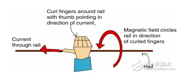
Figure 4: Right-hand rule
Another simple explanation of how RF exists in PCB can be seen from Figures 5 and 6. Here, a typical circuit is analyzed in the time domain and frequency domain. According to Kirchhoff and Ampere’s laws, a closed loop circuit must exist if the circuit is to work. Kirchhoff’s voltage law states that in a circuit, the sum of the voltages around any closed path must be zero. Ampere’s law states that a given current will produce a magnetic induction at a point, which is calculated based on the current unit and the relative position of the current to that point.
If the closed loop circuit does not exist, the signal cannot pass through the transmission line from the source to the load. When the switch is closed, the circuit is established and the AC or DC current begins to flow. In the frequency domain, we regard this current as RF energy. In fact, there are not two different currents (time domain or frequency domain current). There is always only one current, which can be presented in the time domain or frequency domain. An RF return path from the load to the source must also exist, otherwise the circuit will not work. Therefore, the PCB structure must comply with Maxwell’s equations, Kirchhoff’s voltage law, and Ampere’s law.
Maxwell’s equations, Kirchhoff’s and Ampere’s laws all say that for a circuit to work properly or for the desired purpose, a closed loop network must exist. Figure 5 shows such a typical circuit. When a trace reaches the load from the source, a return current path must also exist, which is stipulated by Kirchhoff and Ampere’s laws.
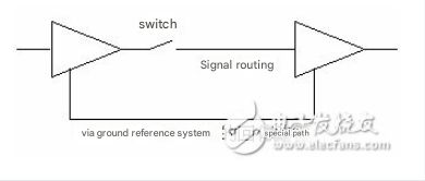
Figure 5: Closed loop circuit
As shown in Figure 6, a switch is connected in series with the source drive end (E). When the switch is closed, the circuit works normally according to the desired result; when the switch is open, it has no function. In the time domain, the desired signal reaches the load from the source. This signal must have a return path to make this circuit valid, which is usually through a 0V (ground) return structure (Kirchhoff’s law). The flow of RF current is from the source to the load, and must return through the path with the lowest possible impedance, usually through a ground trace or ground plane (mirror plane). The existence of RF current is best explained using Ampere’s law.
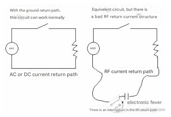
Figure 6: Description of a closed loop circuit
Minimizing magnetic flux
Before discussing “how EMI is generated in PCB”, we must first understand the basic mechanism of “how magnetic flux lines are generated in transmission lines”, because the latter is a basic concept of the former. Magnetic flux lines are generated by a current flowing through a fixed or variable impedance. The impedance in a network
Impedance always exists in traces, component solder wires, vias, etc. If magnetic flux lines exist in the PCB, according to Maaxwell’s equation, various transmission paths for RF energy must also exist. These transmission paths may be radiated through free space or conducted through the interconnection of cables.
In order to eliminate RF currents in the PCB, the concept of “flux cancellation” or “flux minimization” must be introduced first. Because the magnetic flux lines run in the counterclockwise direction in the transmission line, if we make the RF return path parallel and adjacent to the source end trace, the magnetic flux lines on the return path (counterclockwise field) are in the opposite direction compared to the path at the source end (clockwise field). When we combine the clockwise field and the counterclockwise field, a cancellation effect can be produced. If the unwanted magnetic flux lines between the source and the return path can be eliminated or minimized, the radiated or conducted RF current will not exist, except at the very small boundary of the trace. The concept of eliminating magnetic flux is simple, but when designing to eliminate or minimize it, you must pay attention to some pitfalls and easy oversights. Because a small mistake may cause many additional errors, causing more troubleshooting and debugging burdens for EMC engineers. The simplest method of eliminating magnetic flux is to use the “image plane”. No matter how well the PCB layout is designed, magnetic and electric fields will always exist. However, if we eliminate the magnetic flux lines, EMI will not exist. It’s that simple!
How to eliminate magnetic flux lines when designing PCB layout? There are many tips for reference, but not all of them are directly related to eliminating magnetic flux lines. Some of them are briefly described as follows:
●Multilayer boards have correct multilayer settings (stackup assignments) and impedance control.
●Wrap the frequency trace (clock trace) around the return path ground plane (multilayer PCB), ground grid (ground grid), single-sided and double-sided boards can use ground traces, or safe traces (guard trace).
● Reduce the amount of radiation emitted by the component by capturing the magnetic flux lines generated inside the component’s plastic package into a 0V reference system.
● Carefully select logic components to minimize the amount of RF spectrum distribution radiated by the components and traces. Devices with slower edge rates can be used.
● Reduce RF current in the traces by reducing the RF drive voltage (from the frequency generation circuit, such as TTL/CMOS).
● Reduce ground noise voltage, which exists in the power supply and ground plane structures.
● When the maximum capacitive load must be driven and all device pins are switched simultaneously, the component’s decoupling circuit must be sufficient.
● Frequency and signal traces must be properly terminated to avoid ringing, overshoot, and undershoot.
● Use data line filters and common-mode chokes on selected nets.
●When external I/O cables are provided, bypass (non-decoupling) capacitors must be used correctly.
●For components that radiate a lot of common-mode RF energy (generated internally by the component), provide a grounded heat sink.
Looking at the items listed above, we can see that magnetic flux lines are only part of the reason why EMI is generated in the PCB. Other reasons include:
●There are common-mode and differential-mode currents between the circuit and the I/O cable.
●Ground loops create a magnetic field structure.
●Components radiate.
●Impedance mismatch.
Note that most EMI radiation is generated by common-mode levels. These common-mode levels may be transformed into minimal fields in the board or circuit.
Conclusion
To eliminate EMI in the PCB, you must first start by eliminating magnetic flux. However, this is “easier said than done” because RF energy cannot be seen or smelled. However, by finding the location and direction of the RF current, using the techniques described in this article, and referring to Maxwell’s equations, Kirchhoff’s and Ampere’s laws, you can gradually narrow down the suspected area, find the correct EMI location, and eliminate it.