Causes of Copper Voiding in PCB Plated Through Holes: A Comprehensive Analysis
Abstract
Copper voiding in plated through holes (PTHs) of printed circuit boards (PCBs) remains a persistent challenge in the electronics manufacturing industry. This paper examines the root causes of internal copper deficiencies in PCB hole walls, analyzing the complete electroless copper deposition process from material preparation to final plating. We identify seven primary categories of contributing factors: material-related issues, drilling process defects, desmear treatment failures, electroless copper deposition problems, electroplating process shortcomings, environmental and equipment factors, and human operational errors. For each category, we provide detailed technical explanations of failure mechanisms along with corresponding preventive measures. The paper concludes with recommendations for process optimization and quality control improvements to minimize copper void defects in high-reliability PCB manufacturing.
Keywords: PCB manufacturing, plated through holes, copper voiding, electroless copper deposition, electroplating defects
1. Introduction
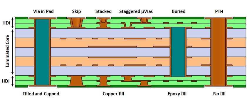
Plated through holes (PTHs) serve as critical conductive pathways in multilayer printed circuit boards, enabling vertical interconnection between different layers. The reliability of these interconnects directly impacts the performance and longevity of electronic devices. Copper voiding—the absence or insufficiency of copper deposition in hole walls—represents one of the most common and detrimental defects in PCB manufacturing. These voids can lead to increased resistance, intermittent connections, or complete circuit open failures, particularly under thermal stress or vibration conditions.
The plating process for through holes involves multiple intricate steps, each presenting potential failure points that may result in copper deficiencies. This paper systematically examines the entire PTH formation process to identify and explain the various causes of internal copper voiding.
2. Material-Related Causes
2.1 Substrate Material Quality
The dielectric material properties significantly influence hole wall plating quality:
- Resin Recession: Poor resin-to-glass bonding in FR-4 materials leads to fiber exposure after drilling, creating uneven surfaces that hinder copper adhesion
- Low Tg Materials: Substrates with glass transition temperatures below 150°C often exhibit excessive thermal expansion during plating, causing copper layer fractures
- Hydrophobic Surfaces: Certain high-frequency materials (e.g., PTFE-based substrates) resist wetting by aqueous solutions, preventing uniform copper deposition
2.2 Copper Foil Issues
- Over-rolled copper foil develops microcracks that propagate during plating
- Inadequate oxide treatment on inner layer copper reduces mechanical interlocking with deposited copper
3. Drilling Process Defects
3.1 Drill Bit Conditions
- Worn drill bits (typically after 500-800 hits) produce rough hole walls with torn fibers and resin smear
- Improper drill geometry (point angle, helix angle) generates excessive heat, causing localized resin melting
3.2 Drilling Parameters
- High spindle speeds (>150 krpm) without proper feed rate adjustment cause thermal degradation
- Insufficient chip load (<0.05 mm/rev) leads to rubbing rather than cutting action
- Inadequate drill retract speed results in debris redeposition on hole walls
3.3 Debris Management
- Ineffective vacuum systems fail to remove drilling debris (up to 30% of holes may contain residual debris)
- Coolant contamination with oils or particulates leaves hydrophobic residues
4. Desmear and Cleaning Process Failures
4.1 Smear Removal Incompleteness
- Insufficient permanganate concentration (<60 g/L) or temperature (<75°C) in desmear baths
- Short process time (<5 minutes) for thick multilayer boards (>12 layers)
- Inadequate neutralization after oxidative desmear leaves active sites unactivated
4.2 Microetching Problems
- Over-etching (>1.5 μm copper removal) creates excessive surface roughness
- Under-etching (<0.3 μm) fails to provide adequate bonding sites
- Contaminated microetch solutions (Cu²+ >25 g/L) produce passivated surfaces
4.3 Cleaning Deficiencies
- Drag-out from previous baths contaminates subsequent processes
- Deionized water with high resistivity (>1 MΩ·cm) carries away surfactants prematurely
- Inadequate rinsing (<30 seconds immersion time) leaves process chemicals in holes
5. Electroless Copper Deposition Issues
5.1 Catalyzation Defects
- Palladium colloid agglomeration (particles >0.1 μm) causes uneven activation
- Sensitizer exhaustion (Sn²+ <2 g/L) results in sparse catalytic sites
- Cross-contamination with complexing agents deactivates catalytic centers
5.2 Electroless Plating Problems
- Bath imbalance (formaldehyde <6 mL/L or NaOH <8 g/L) slows deposition rate
- Excessive stabilizer concentration (>50 ppm) causes bath over-suppression
- Particulate contamination (>5 μm particles) creates shadow areas
- Gas bubble entrapment in high aspect ratio holes (>8:1) blocks copper deposition
5.3 Deposit Quality
- Thin initial coating (<0.3 μm) cannot withstand subsequent electroplating stresses
- Poor adhesion (peel strength <1 N/mm) leads to copper separation during thermal cycling
6. Electroplating Process Shortcomings
6.1 Current Distribution
- Poor throwing power (<70% in 8:1 aspect ratio holes) creates center voids
- Incorrect anode-to-cathode ratio (<1:1 for high aspect ratio holes)
- Insufficient agitation (solution flow <0.5 m/s in holes) causes ion depletion
6.2 Bath Chemistry
- Organic additives imbalance (carrier:suppressor:accelerator ratio deviation >15%)
- Copper ion concentration fluctuation (beyond 60±5 g/L range)
- Chloride ion control failure (outside 50-80 ppm optimal range)
6.3 Process Control
- Rack plating with poor contact resistance (>10 mΩ per contact point)
- Pulse reverse plating with improper parameters (ton:toff ratio mismatch)
- Bath temperature variation (>±2°C from setpoint)
7. Environmental and Equipment Factors
7.1 Facility Conditions
- Airborne particulates (>Class 10,000 cleanroom) settling on panels
- Temperature fluctuations (>±5°C/hour) causing bath performance variations
- Humidity control failure (RH >60%) promoting oxide formation
7.2 Equipment Issues
- Filter system failures (>10 psi differential pressure)
- Pump cavitation causing flow irregularities
- Anode bag ruptures releasing particles
- Rectifier ripple (>5%) creating uneven deposition
8. Human Factors and Operational Errors
8.1 Process Deviation
- Shortcutting prescribed immersion times
- Improper racking techniques causing shadowing
- Incorrect bath replenishment calculations
8.2 Maintenance Lapses
- Delayed anode replacement (after >3,000 Ah/L throughput)
- Inadequate tank cleaning frequency
- Poor record keeping of bath analyses
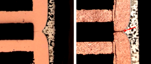
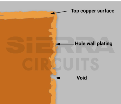
9. Detection and Analysis Methods
9.1 Non-Destructive Testing
- Automated optical inspection (AOI) with 10 μm resolution
- X-ray tomography for 3D void mapping
- Thermal imaging for latent adhesion defects
9.2 Destructive Analysis
- Cross-sectioning with precision polishing
- Scanning electron microscopy (SEM) of interface quality
- Energy dispersive spectroscopy (EDS) for contamination identification
10. Preventive Measures and Best Practices
10.1 Process Optimization
- Implement statistical process control (SPC) for critical parameters
- Establish golden samples for visual benchmarks
- Develop customized process recipes for different material types
10.2 Quality Control Enhancements
- Regular bath analysis (every 4 hours for electroless copper)
- Monthly equipment performance verification
- Annual process capability (Cpk) studies
10.3 Staff Training
- Certification programs for plating operators
- Cross-training between engineering and production
- Failure analysis workshops
11. Conclusion
Copper voiding in PCB through holes stems from multifaceted causes spanning material selection, process execution, equipment maintenance, and human factors. Successful prevention requires holistic process control incorporating:
- Rigorous material qualification protocols
- Precision drilling parameter optimization
- Meticulous chemical process monitoring
- Comprehensive equipment maintenance programs
- Continuous operator training initiatives
Implementing these measures can reduce copper void defects to below 50 ppm levels, significantly enhancing PCB reliability. Future research directions should focus on real-time monitoring systems and advanced plating chemistry formulations to further improve PTH quality.


