Causes of PCB Pad Lifting and Poor Solderability: A Comprehensive Analysis
Introduction
Printed Circuit Board (PCB) reliability is critical in electronic manufacturing, with pad integrity being one of the most fundamental requirements. Pad lifting (where copper pads separate from the PCB substrate) and poor solderability (difficulty in achieving proper solder wetting) represent two common yet serious issues in PCB assembly. These problems can lead to open circuits, intermittent connections, and ultimately product failures. This article examines the root causes of these phenomena, covering material selection, manufacturing processes, design considerations, and environmental factors that contribute to pad reliability issues.
Section 1: Fundamental Causes of PCB Pad Lifting
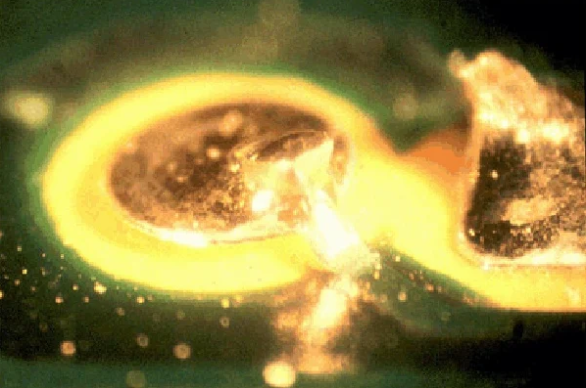
1.1 Adhesion Failure Between Copper and Substrate
The bond between copper pads and the PCB substrate (typically FR-4) depends on proper surface treatment and adhesive properties. Several factors can compromise this bond:
- Inadequate surface preparation: Improper cleaning or treatment of the substrate before copper application weakens adhesion
- Oxidation contamination: Presence of oxides or other contaminants at the interface
- Thermal stress mismatch: Differences in thermal expansion coefficients between copper and substrate materials
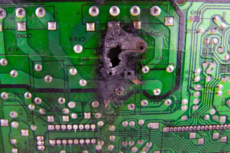
- Mechanical stress: Excessive mechanical forces during drilling, routing, or handling
1.2 Thermal Stress During Soldering
Soldering operations subject PCB pads to significant thermal stress:
- Reflow soldering temperatures (typically 220-260°C) approach the glass transition temperature (Tg) of many substrates
- Thermal cycling during multiple rework operations accumulates stress
- Localized overheating from soldering irons or hot air tools can degrade the pad-substrate bond
- Rapid temperature changes cause differential expansion between materials
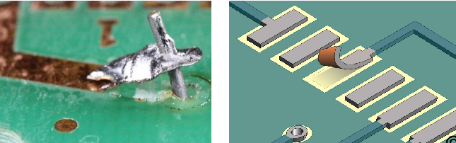
1.3 Mechanical Stress Factors
Physical forces contribute significantly to pad lifting:
- Excessive solder wick removal force during rework
- Component lead bending stress after soldering
- Vibration and shock in end-use environments
- Improper handling with tools that pry against pads
1.4 Material Selection Issues
Choice of materials affects pad adhesion:
- Low-Tg substrates soften at normal soldering temperatures
- Poor quality copper foil with inadequate tooth profile for mechanical bonding
- Incompatible adhesives in copper-clad laminates
- Moisture absorption in substrate materials leading to steam pressure during soldering
Section 2: Root Causes of Poor Solderability
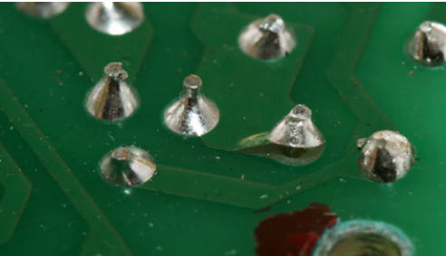
2.1 Surface Oxidation and Contamination
Copper surfaces must be clean and oxide-free for proper solder wetting:
- Atmospheric oxidation: Exposure to air forms copper oxides that resist solder wetting
- Process contaminants: Oils, fingerprints, flux residues, or other processing chemicals
- Storage conditions: High humidity or corrosive atmospheres accelerate oxidation
- Excessive time between fabrication and assembly allows oxidation buildup
2.2 Improper Surface Finishes
Common PCB surface finishes affect solderability differently:
- HASL (Hot Air Solder Leveling): Can oxidize over time; uneven surfaces may cause wetting issues
- ENIG (Electroless Nickel Immersion Gold): Black pad syndrome from poor nickel plating; gold too thin or too thick
- Immersion Silver: Tarnishing or sulfur contamination; organic solderability preservative (OSP) degradation
- Electrolytic Hard Gold: Requires nickel underlayer; excessive gold thickness leads to embrittlement
2.3 Flux-Related Issues
Flux performance directly impacts solderability:
- Insufficient flux activity for the oxide level present
- Wrong flux type (water-soluble vs. no-clean vs. rosin)
- Flux expiration or degradation
- Inadequate flux application quantity or coverage
2.4 Soldering Process Parameters
Process control affects solderability outcomes:
- Temperature profiles (insufficient preheat or peak temperature)
- Time above liquidus too short for proper wetting
- Atmosphere control (oxidation in air vs. nitrogen)
- Solder alloy composition and contamination
Section 3: Design and Manufacturing Factors
3.1 PCB Design Considerations
Design choices influence pad reliability:
- Pad size relative to component lead: Too small reduces mechanical strength
- Thermal relief design: Poor designs create uneven heating
- Copper weight and thickness: Thin copper more prone to lifting
- Annular ring adequacy: Minimal rings drill easily
3.2 Fabrication Process Controls
Manufacturing variables affect pad quality:
- Drilling parameters: Excessive heat or vibration damages pad adhesion
- Plating quality: Thin or porous copper in through-holes
- Lamination conditions: Incomplete curing of substrate materials
- Cleanliness controls: Residual etchant or drilling debris
3.3 Environmental Exposure
Storage and operating environments impact pads:
- Humidity absorption by PCB materials
- Corrosive atmospheres (industrial, marine environments)
- Temperature cycling in storage or operation
- UV exposure degrading surface finishes
Section 4: Prevention and Mitigation Strategies
4.1 Material Selection Best Practices
- Specify high-Tg materials for lead-free processing
- Require certified copper foil with proper roughness
- Select appropriate surface finishes for application
- Verify laminate supplier quality controls
4.2 Design Guidelines for Pad Reliability
- Adequate annular rings for through-hole components
- Thermal relief patterns that distribute stress
- Pad sizes matched to component requirements
- Avoidance of pads on bend lines or high-stress areas
4.3 Process Control Measures
- Controlled soldering parameters with profile verification
- Proper handling procedures to prevent mechanical damage
- Nitrogen atmosphere for critical soldering operations
- First-article inspection of solderability
4.4 Storage and Handling Protocols
- Dry storage with humidity control
- Limited shelf life for sensitive finishes like OSP
- Proper packaging to prevent mechanical damage
- Baking procedures for moisture-laden boards
Conclusion
PCB pad lifting and poor solderability stem from complex interactions between materials, design, manufacturing processes, and environmental factors. Addressing these issues requires a systematic approach across the entire product lifecycle—from material selection through design, fabrication, assembly, and field use. By understanding the root causes outlined in this analysis, engineers can implement appropriate prevention strategies to enhance PCB reliability. Continuous improvement in substrate materials, surface finishes, and process controls continues to reduce these failure modes in modern electronic manufacturing.