Causes of Warpage in PCB Manufacturing Process
Abstract
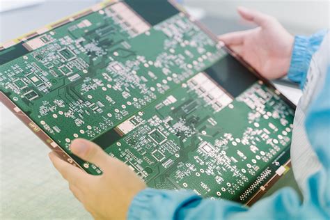
Printed Circuit Boards (PCBs) are essential components in modern electronics, but warpage (curvature or twisting of the board) is a common issue during manufacturing. Warpage can lead to assembly defects, poor solder joint reliability, and even device failure. This paper explores the key factors contributing to PCB warpage, including material selection, thermal stress, lamination processes, copper distribution, and environmental conditions. Mitigation strategies are also briefly discussed to minimize warpage-related defects.
1. Introduction
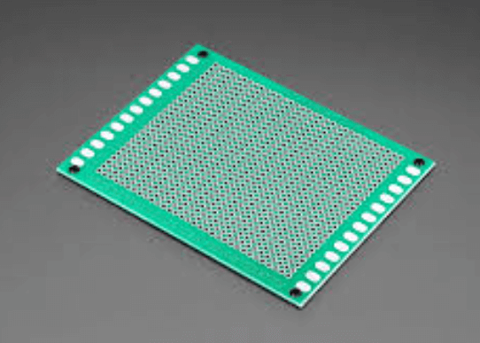
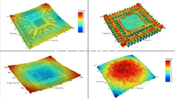
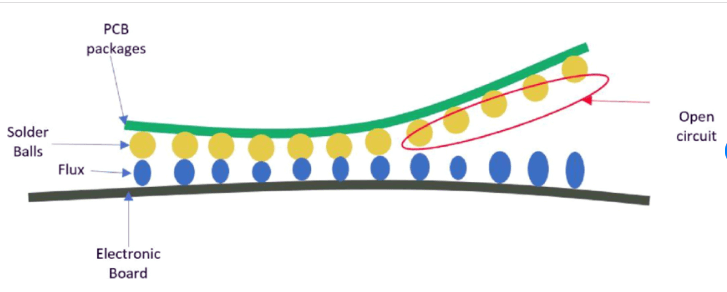
PCB warpage refers to the undesired bending or twisting of a circuit board, which can cause misalignment during surface mount technology (SMT) assembly, solder bridging, or open circuits. Excessive warpage (typically beyond 0.75% of the board length) can lead to significant manufacturing challenges. Understanding the root causes of warpage is crucial for improving PCB reliability and yield.

2. Primary Causes of PCB Warpage
2.1 Material Selection and Properties
The choice of base materials significantly impacts PCB flatness:
- CTE Mismatch: The Coefficient of Thermal Expansion (CTE) of the substrate (e.g., FR-4, polyimide) and copper layers must be balanced. If the CTE difference is too large, heating or cooling induces stress, leading to warpage.
- Glass Transition Temperature (Tg): High-Tg materials (e.g., FR-4 Tg170) resist deformation at elevated temperatures but may still warp if cooling rates are uneven.
- Prepreg Resin Content: Improper resin-to-glass fiber ratios in prepreg layers can cause asymmetric expansion.
2.2 Thermal Stress During Manufacturing
PCBs undergo multiple heating cycles during fabrication:
- Lamination Process: High pressure and temperature during lamination can cause residual stress if cooling is non-uniform. Rapid cooling exacerbates warpage.
- Solder Reflow: Repeated exposure to reflow temperatures (e.g., lead-free reflow at 250°C) can induce warpage, especially in thin or large PCBs.
- Uneven Heating: Localized heating during processes like hot air solder leveling (HASL) may create thermal gradients that deform the board.
2.3 Copper Distribution Imbalance
Copper layers provide mechanical support, and uneven copper distribution leads to asymmetric stresses:
- Copper Thickness Variations: Heavy copper on one side and light copper on the other creates tension differences.
- Copper Pattern Density: Large copper planes versus sparse traces can cause differential expansion.
- Inner Layer Design: Poorly balanced copper weights in multilayer PCBs increase warpage risk.
2.4 Lamination and Layer Stackup Issues
Multilayer PCBs are prone to warpage due to layer stackup inconsistencies:
- Asymmetric Stackup: Uneven layer counts or material types on either side of the neutral axis induce bending.
- Prepreg Misalignment: Improperly aligned prepreg layers create internal stresses.
- Resin Flow Imbalance: Excessive or insufficient resin flow during lamination affects dimensional stability.
2.5 Moisture Absorption
PCB materials (e.g., FR-4) are hygroscopic and absorb moisture from the environment:
- Swelling Effects: Absorbed moisture expands during heating, causing temporary or permanent warpage.
- Baking Requirements: Inadequate pre-baking before reflow can lead to moisture-related deformation (“popcorn effect”).
2.6 Mechanical and Environmental Stress
External factors also contribute to warpage:
- Handling and Storage: Mechanical stress during transport or storage can deform PCBs.
- Environmental Humidity: High humidity levels exacerbate moisture absorption.
- Panelization and Routing: Improper panel support or routing techniques may introduce stress.
3. Mitigation Strategies
To minimize warpage, manufacturers employ several techniques:
- Balanced Copper Distribution: Symmetric copper weights and patterns across layers.
- Optimized Lamination Process: Controlled cooling rates and pressure during lamination.
- Material Selection: Using high-Tg, low-CTE, or flexible materials for demanding applications.
- Moisture Control: Proper storage in dry environments and pre-baking before assembly.
- Stiffeners and Carriers: Additional support for thin or large PCBs during reflow.
4. Conclusion
PCB warpage is a multifactorial issue influenced by material properties, thermal stresses, copper balance, lamination processes, and environmental conditions. By understanding these causes, manufacturers can implement design and process optimizations to reduce warpage and enhance PCB reliability. Future advancements in materials and process controls will further mitigate this challenge.