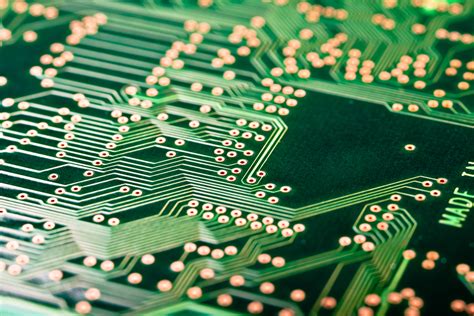
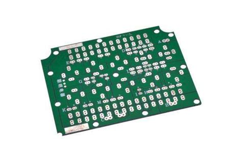
Ceramic inlay pcb
Advantages Of Ceramic Inlay PCB In High-Frequency Applications
Ceramic inlay PCBs have emerged as a pivotal innovation in the realm of high-frequency applications, offering a multitude of advantages that make them indispensable in various advanced technological fields.
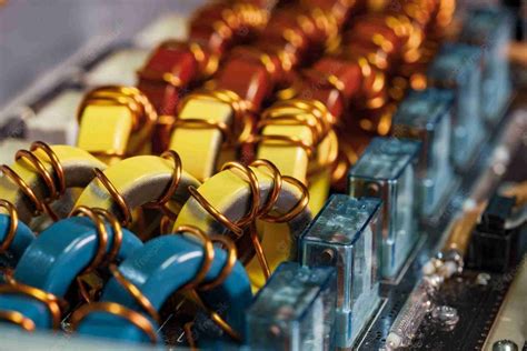
One of the primary benefits of ceramic inlay PCBs is their exceptional thermal conductivity.
Unlike traditional PCBs, which often struggle with heat dissipation, ceramic inlay PCBs efficiently manage thermal loads, thereby enhancing the overall performance and reliability of electronic devices. This superior thermal management is particularly crucial in high-frequency applications where excessive heat can lead to signal degradation and component failure.
In addition to their thermal properties, ceramic inlay PCBs exhibit remarkable electrical insulation.
The ceramic material used in these PCBs provides a high dielectric strength, which is essential for maintaining signal integrity in high-frequency circuits. This characteristic ensures that the signals transmitted through the PCB remain clear and free from interference, thereby improving the overall efficiency and performance of the electronic system. Furthermore, the low dielectric constant of ceramic materials minimizes signal loss, making ceramic inlay PCBs an ideal choice for applications that require precise and reliable signal transmission.
Moreover, the mechanical stability of ceramic inlay PCBs cannot be overstated. These PCBs are highly resistant to mechanical stress and environmental factors such as moisture and temperature fluctuations.
This robustness ensures that the PCBs maintain their structural integrity and functionality even in harsh operating conditions. Consequently, ceramic inlay PCBs are widely used in aerospace, military, and automotive industries, where reliability and durability are paramount.
Another significant advantage of ceramic inlay PCBs is their compatibility with advanced manufacturing processes. The use of ceramic materials allows for the integration of fine-pitch components and high-density interconnects, which are essential for modern high-frequency applications.
This compatibility not only enhances the performance of the electronic devices but also enables the miniaturization of circuits, leading to more compact and efficient designs. As a result, ceramic inlay PCBs are increasingly being adopted in the development of next-generation communication systems, medical devices, and consumer electronics.
Furthermore, the environmental benefits of ceramic inlay PCBs are worth mentioning. Ceramic materials are inherently non-toxic and environmentally friendly, making them a sustainable choice for PCB manufacturing.
This aspect aligns with the growing emphasis on green technologies and sustainable practices in the electronics industry. By opting for ceramic inlay PCBs, manufacturers can reduce their environmental footprint while still achieving high performance and reliability in their products.
In conclusion, the advantages of ceramic inlay PCBs in high-frequency applications are manifold. Their superior thermal conductivity, excellent electrical insulation, mechanical stability, compatibility with advanced manufacturing processes, and environmental benefits make them a preferred choice for a wide range of industries. As technology continues to evolve and the demand for high-frequency applications grows, the adoption of ceramic inlay PCBs is likely to increase, driving further innovation and advancements in electronic design and manufacturing.
Manufacturing Process Of Ceramic Inlay PCB
The manufacturing process of ceramic inlay PCBs is a sophisticated and intricate procedure that demands precision and expertise. Ceramic inlay PCBs are renowned for their superior thermal management, high-frequency performance, and exceptional reliability, making them indispensable in advanced electronic applications. The journey from raw materials to a fully functional ceramic inlay PCB involves several meticulously coordinated steps, each contributing to the final product’s quality and performance.
To begin with, the selection of materials is paramount.
High-purity ceramic substrates, typically alumina or aluminum nitride, are chosen for their excellent thermal conductivity and electrical insulation properties. These substrates form the foundation upon which the entire PCB is built. The initial step involves cutting the ceramic material into the desired dimensions, ensuring that the substrate is free from any defects or impurities that could compromise the PCB’s performance.
Following the preparation of the ceramic substrate, the next phase involves the application of a conductive layer.
This is achieved through a process known as screen printing, where a conductive paste, usually composed of silver or copper, is meticulously applied to the substrate. The paste is then subjected to a high-temperature firing process, which solidifies the conductive material and ensures a robust bond with the ceramic substrate. This step is crucial as it forms the electrical pathways that will interconnect the various components of the PCB.
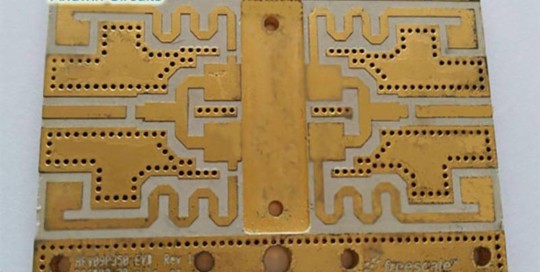
Once the conductive layer is in place, the focus shifts to the creation of the inlay.
The inlay process involves embedding additional materials, such as copper or other metals, into the ceramic substrate to enhance its electrical and thermal properties. This is typically done using a technique called laser drilling, where precise holes are created in the ceramic substrate. These holes are then filled with the chosen metal, which is subsequently bonded to the substrate through a process of high-temperature sintering. This ensures a seamless integration of the inlay material with the ceramic base, resulting in a PCB that boasts superior performance characteristics.
The next stage in the manufacturing process is the application of the dielectric layer.
This layer serves to insulate the various conductive pathways and prevent any unintended electrical interactions. The dielectric material is carefully selected to match the thermal expansion properties of the ceramic substrate, ensuring that the PCB remains stable under varying thermal conditions. The dielectric layer is applied using advanced deposition techniques, such as chemical vapor deposition (CVD) or physical vapor deposition (PVD), which guarantee a uniform and defect-free coating.
Following the application of the dielectric layer, the PCB undergoes a series of precision machining processes.
These include drilling, routing, and milling, which are performed using state-of-the-art CNC machines. These processes are essential for creating the intricate patterns and structures required for the final PCB design. The machining phase is followed by a thorough cleaning process to remove any residual debris or contaminants that could affect the PCB’s performance.
Finally, the ceramic inlay PCB undergoes a rigorous testing and inspection phase. This includes electrical testing to verify the integrity of the conductive pathways, as well as thermal cycling tests to ensure the PCB can withstand extreme temperature variations. Any defects or inconsistencies are identified and rectified at this stage, ensuring that only the highest quality PCBs make it to the final assembly line.
In conclusion, the manufacturing process of ceramic inlay PCBs is a complex and highly specialized procedure that demands precision at every step. From material selection and conductive layer application to inlay integration and final testing, each phase is meticulously executed to produce PCBs that meet the highest standards of performance and reliability. This intricate process underscores the critical role that ceramic inlay PCBs play in advancing modern electronic technologies.
Thermal Management Benefits Of Ceramic Inlay PCB
Ceramic inlay PCBs have emerged as a significant advancement in the realm of printed circuit board technology, particularly in applications where thermal management is a critical concern.
These specialized PCBs incorporate ceramic materials, which are renowned for their exceptional thermal conductivity and electrical insulation properties. As electronic devices continue to shrink in size while increasing in power density, the need for efficient thermal management solutions has never been more pressing. Ceramic inlay PCBs offer a compelling solution to this challenge, providing numerous thermal management benefits that enhance the performance and reliability of electronic systems.
One of the primary advantages of ceramic inlay PCBs is their superior thermal conductivity.
Traditional PCBs, typically made from materials like FR4, have limited thermal conductivity, which can lead to overheating and potential failure of electronic components. In contrast, ceramic materials such as aluminum oxide (Al2O3) and aluminum nitride (AlN) used in ceramic inlay PCBs exhibit much higher thermal conductivity. This allows for more efficient heat dissipation from high-power components, thereby reducing the risk of thermal damage and extending the lifespan of the device.
Moreover, ceramic inlay PCBs offer excellent thermal stability, which is crucial for maintaining consistent performance in varying environmental conditions.
Unlike conventional PCBs, which can suffer from thermal expansion and contraction, ceramic materials exhibit minimal thermal expansion. This stability ensures that the PCB maintains its structural integrity and electrical performance even under extreme temperature fluctuations. Consequently, electronic devices that utilize ceramic inlay PCBs are better equipped to operate reliably in harsh environments, such as automotive, aerospace, and industrial applications.
In addition to their thermal conductivity and stability, ceramic inlay PCBs also provide enhanced electrical insulation.
The ceramic materials used in these PCBs possess high dielectric strength, which prevents electrical breakdown and ensures reliable operation of the electronic components. This is particularly important in high-voltage applications, where electrical insulation is critical to prevent short circuits and other electrical failures. By combining excellent thermal management with robust electrical insulation, ceramic inlay PCBs offer a comprehensive solution for high-performance electronic systems.
Furthermore, the integration of ceramic inlays into PCBs allows for greater design flexibility.
Engineers can strategically place ceramic inlays in areas where heat generation is most significant, optimizing the thermal management of the entire system. This targeted approach not only improves the overall thermal performance but also enables the design of more compact and efficient electronic devices. As a result, manufacturers can develop smaller, lighter, and more powerful products without compromising on reliability or performance.
The benefits of ceramic inlay PCBs extend beyond thermal management to include improved mechanical strength and durability.
Ceramic materials are inherently robust and resistant to wear and tear, making them ideal for applications that demand high reliability and longevity. This durability ensures that electronic devices can withstand mechanical stresses and environmental challenges, further enhancing their overall performance and lifespan.
In conclusion, ceramic inlay PCBs represent a significant advancement in PCB technology, offering unparalleled thermal management benefits that are essential for modern electronic systems. Their superior thermal conductivity, stability, electrical insulation, design flexibility, and mechanical strength make them an ideal choice for high-performance applications across various industries. As the demand for more powerful and compact electronic devices continues to grow, ceramic inlay PCBs will undoubtedly play a crucial role in meeting these challenges and driving innovation in the field of electronics.
Comparing Ceramic Inlay PCB To Traditional PCB Materials
When it comes to the world of printed circuit boards (PCBs), the choice of material can significantly impact the performance, durability, and overall efficiency of the final product. Among the various materials available, ceramic inlay PCBs have emerged as a noteworthy alternative to traditional PCB materials such as FR4, polyimide, and metal-core substrates. To understand the advantages and potential drawbacks of ceramic inlay PCBs, it is essential to compare them with their conventional counterparts.
One of the most striking differences between ceramic inlay PCBs and traditional PCB materials lies in their thermal management capabilities.
Ceramic materials, such as aluminum oxide (Al2O3) and aluminum nitride (AlN), possess excellent thermal conductivity properties. This allows ceramic inlay PCBs to dissipate heat more effectively, making them ideal for high-power applications where thermal management is critical. In contrast, traditional materials like FR4 have relatively poor thermal conductivity, which can lead to overheating and reduced performance in demanding environments.
In addition to superior thermal management, ceramic inlay PCBs offer enhanced mechanical stability.
The inherent rigidity and strength of ceramic materials provide a robust foundation that can withstand mechanical stress and environmental factors such as vibration and temperature fluctuations. This makes ceramic inlay PCBs particularly suitable for applications in aerospace, automotive, and industrial sectors, where reliability and durability are paramount. On the other hand, traditional PCB materials may exhibit greater flexibility but often lack the same level of mechanical resilience, potentially leading to issues such as warping or delamination over time.
Another critical aspect to consider is the electrical performance of ceramic inlay PCBs compared to traditional materials.
Ceramic substrates exhibit low dielectric loss and high dielectric strength, which translates to better signal integrity and reduced electromagnetic interference (EMI). This is particularly advantageous in high-frequency applications, such as RF and microwave circuits, where maintaining signal fidelity is crucial. Traditional materials, while adequate for many applications, may not offer the same level of electrical performance, potentially limiting their use in high-frequency or high-speed circuits.
Despite these advantages, it is important to acknowledge that ceramic inlay PCBs are not without their challenges.
One of the primary concerns is the cost associated with ceramic materials and the manufacturing processes involved. Ceramic substrates are generally more expensive than traditional materials, which can increase the overall cost of the PCB. Additionally, the fabrication of ceramic inlay PCBs requires specialized equipment and techniques, which may not be readily available in all manufacturing facilities. This can lead to longer lead times and higher production costs, potentially limiting their adoption in cost-sensitive applications.
Furthermore, while ceramic inlay PCBs offer excellent thermal and mechanical properties, they may not be the best choice for all applications. For instance, in scenarios where flexibility is a key requirement, such as in wearable electronics or flexible displays, traditional materials like polyimide may be more suitable. The rigid nature of ceramic substrates can be a limitation in these contexts, highlighting the importance of selecting the appropriate material based on the specific needs of the application.
In conclusion, ceramic inlay PCBs present a compelling alternative to traditional PCB materials, offering superior thermal management, mechanical stability, and electrical performance. However, the higher cost and specialized manufacturing requirements associated with ceramic substrates must be carefully considered. By weighing the advantages and potential drawbacks, engineers and designers can make informed decisions to optimize the performance and reliability of their electronic products.