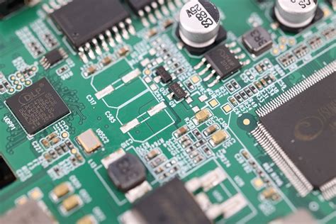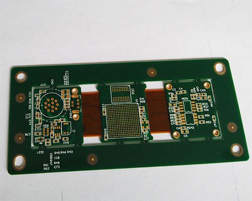
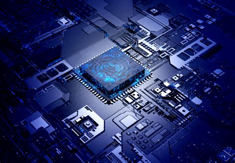
Ceramic pcb material
Advantages Of Ceramic PCB Material In High-Frequency Applications
Ceramic printed circuit boards (PCBs) have emerged as a pivotal component in the realm of high-frequency applications, offering a multitude of advantages that make them an ideal choice for various industries. As technology continues to advance, the demand for materials that can withstand high frequencies and deliver superior performance has become increasingly critical. Ceramic PCBs, with their unique properties, have proven to be highly effective in meeting these demands, thereby gaining prominence in sectors such as telecommunications, aerospace, and automotive industries.
One of the primary advantages of ceramic PCB material is its excellent thermal conductivity.
In high-frequency applications, managing heat dissipation is crucial to ensure the reliability and longevity of electronic components. Ceramic materials, such as aluminum oxide and aluminum nitride, possess high thermal conductivity, which allows for efficient heat transfer away from the components. This property significantly reduces the risk of overheating, thereby enhancing the overall performance and durability of the electronic devices.
In addition to thermal management, ceramic PCBs offer superior electrical insulation.
The dielectric properties of ceramic materials are particularly beneficial in high-frequency applications, where maintaining signal integrity is paramount. The low dielectric constant and loss tangent of ceramics minimize signal loss and ensure that high-frequency signals are transmitted with minimal distortion. This characteristic is especially important in applications such as radio frequency (RF) communication systems, where signal clarity and precision are essential.
Moreover, ceramic PCBs exhibit exceptional mechanical strength and stability.
Unlike traditional PCB materials such as FR-4, ceramics are inherently more robust and resistant to mechanical stress. This durability makes ceramic PCBs suitable for use in harsh environments, where they may be subjected to extreme temperatures, vibrations, and other challenging conditions. The mechanical stability of ceramic materials ensures that the PCBs maintain their structural integrity, thereby reducing the likelihood of failure and extending the lifespan of the electronic devices.
Furthermore, ceramic PCBs are known for their excellent chemical resistance.
In high-frequency applications, electronic components may be exposed to various chemicals and corrosive substances. Ceramic materials are inherently resistant to chemical degradation, providing an added layer of protection for the PCBs. This resistance to chemical attack ensures that the performance of the electronic devices remains uncompromised, even in demanding environments.
Another noteworthy advantage of ceramic PCB material is its ability to support miniaturization.
As electronic devices continue to shrink in size, the need for compact and efficient components becomes increasingly important. Ceramic PCBs can be manufactured with high precision, allowing for the integration of complex circuitry in a smaller footprint. This capability is particularly advantageous in applications such as mobile devices and wearable technology, where space is at a premium.
In conclusion, the advantages of ceramic PCB material in high-frequency applications are manifold.
From superior thermal conductivity and electrical insulation to exceptional mechanical strength and chemical resistance, ceramic PCBs offer a comprehensive solution for the challenges posed by high-frequency environments. As industries continue to push the boundaries of technology, the role of ceramic PCBs in ensuring reliable and efficient performance will undoubtedly become even more significant. Consequently, the adoption of ceramic PCB material is poised to grow, driven by the ever-increasing demand for high-performance electronic components in a wide array of applications.
Thermal Management Solutions Using Ceramic PCB Material
In the realm of electronic design and manufacturing, thermal management is a critical consideration, particularly as devices become more compact and powerful.
One innovative solution that has gained prominence is the use of ceramic printed circuit board (PCB) material. Ceramic PCBs offer a range of benefits that make them an attractive option for managing heat in electronic applications, especially when compared to traditional materials like FR-4.
Ceramic materials, such as aluminum oxide (Al2O3), aluminum nitride (AlN), and beryllium oxide (BeO), are known for their excellent thermal conductivity.
This property is crucial in applications where heat dissipation is a priority, as it allows for efficient transfer of heat away from sensitive components. By facilitating rapid heat dissipation, ceramic PCBs help maintain optimal operating temperatures, thereby enhancing the reliability and longevity of electronic devices. This is particularly important in high-power applications, such as LED lighting, power electronics, and RF modules, where excessive heat can lead to performance degradation or even failure.
Moreover, ceramic PCBs exhibit superior mechanical strength and stability compared to their traditional counterparts.
This robustness is beneficial in environments subject to mechanical stress or thermal cycling, where materials are exposed to repeated heating and cooling. The inherent stability of ceramic materials ensures that the PCB maintains its structural integrity, reducing the risk of warping or cracking over time. Consequently, devices utilizing ceramic PCBs can operate reliably in harsh conditions, making them suitable for aerospace, automotive, and industrial applications.
In addition to their thermal and mechanical advantages, ceramic PCBs offer excellent electrical insulation properties.
This characteristic is essential for preventing electrical interference and ensuring signal integrity in high-frequency applications. The low dielectric constant and loss tangent of ceramic materials contribute to minimal signal loss, making them ideal for high-speed and high-frequency circuits. As a result, ceramic PCBs are increasingly used in telecommunications and microwave applications, where maintaining signal quality is paramount.
Despite these advantages, the adoption of ceramic PCBs is not without challenges.
One of the primary considerations is cost. Ceramic materials and the processes involved in manufacturing ceramic PCBs can be more expensive than traditional options. However, the long-term benefits, such as improved performance and reliability, often justify the initial investment, particularly in applications where failure is not an option.
Furthermore, advancements in manufacturing techniques are gradually reducing the cost barrier.
Innovations such as low-temperature co-fired ceramics (LTCC) and high-temperature co-fired ceramics (HTCC) have streamlined the production process, making ceramic PCBs more accessible to a broader range of industries. These techniques allow for the integration of multiple layers and components within a single ceramic substrate, further enhancing the functionality and compactness of electronic devices.
In conclusion, ceramic PCB material represents a significant advancement in thermal management solutions for electronic applications. Its superior thermal conductivity, mechanical strength, and electrical insulation properties make it an ideal choice for high-power, high-frequency, and harsh environment applications. While cost considerations remain, ongoing advancements in manufacturing processes are making ceramic PCBs increasingly viable for a wide array of industries. As electronic devices continue to evolve, the role of ceramic PCBs in ensuring their performance and reliability is likely to expand, solidifying their place as a cornerstone of modern electronic design.
Comparing Ceramic PCB Material With Traditional FR4 Substrates
Ceramic PCB materials have emerged as a significant alternative to traditional FR4 substrates, offering distinct advantages that cater to specific applications in the electronics industry. As technology advances, the demand for materials that can withstand higher temperatures and provide superior thermal management has increased, making ceramic PCBs an attractive option. To understand the benefits and limitations of ceramic PCB materials compared to traditional FR4 substrates, it is essential to explore their properties, applications, and performance characteristics.
Ceramic PCBs are primarily composed of materials such as aluminum oxide (Al2O3), aluminum nitride (AlN), and beryllium oxide (BeO).
These materials are known for their excellent thermal conductivity, which is a critical factor in applications where heat dissipation is crucial. In contrast, FR4 substrates, which are made from woven fiberglass cloth with an epoxy resin binder, have relatively low thermal conductivity.
This difference in thermal performance makes ceramic PCBs particularly suitable for high-power applications, such as LED lighting, power electronics, and RF modules, where efficient heat management is essential to maintain performance and reliability.
Moreover, ceramic materials exhibit superior mechanical strength and stability compared to FR4 substrates
This robustness allows ceramic PCBs to withstand harsh environmental conditions, including high temperatures and mechanical stress, without compromising their structural integrity. Consequently, ceramic PCBs are often used in aerospace, automotive, and military applications, where durability and reliability are paramount. On the other hand, FR4 substrates, while adequate for many consumer electronics, may not offer the same level of performance in extreme conditions.
In addition to thermal and mechanical advantages, ceramic PCBs also provide excellent electrical insulation properties.
This characteristic is particularly beneficial in high-frequency applications, where minimizing signal loss and interference is critical. The low dielectric constant and loss tangent of ceramic materials contribute to improved signal integrity, making them ideal for RF and microwave circuits. Conversely, FR4 substrates, with their higher dielectric constant, may not perform as well in these high-frequency scenarios, potentially leading to signal degradation.
Despite these advantages, ceramic PCBs are not without their limitations.
One of the primary challenges associated with ceramic materials is their higher cost compared to FR4 substrates. The manufacturing process for ceramic PCBs is more complex and requires specialized equipment, which can result in increased production costs.
This factor may limit their use in cost-sensitive applications where the benefits of ceramic materials do not justify the additional expense. Furthermore, the brittleness of ceramic materials can pose challenges during handling and assembly, necessitating careful consideration in the design and manufacturing processes.
In conclusion, while ceramic PCB materials offer significant advantages over traditional FR4 substrates in terms of thermal management, mechanical strength, and electrical insulation, they also present challenges related to cost and brittleness.
The choice between ceramic and FR4 substrates ultimately depends on the specific requirements of the application, including performance, environmental conditions, and budget constraints. As the electronics industry continues to evolve, the demand for materials that can meet increasingly stringent performance criteria will likely drive further innovation and adoption of ceramic PCBs in specialized applications. By carefully weighing the benefits and limitations of each material, engineers and designers can make informed decisions that optimize the performance and reliability of their electronic products.
Innovations In Ceramic PCB Material For Miniaturized Electronics
The rapid advancement of technology has necessitated the development of innovative materials to support the miniaturization of electronic devices.
Among these materials, ceramic printed circuit boards (PCBs) have emerged as a pivotal component in the evolution of miniaturized electronics. Ceramic PCBs are increasingly favored for their superior thermal management, electrical insulation, and mechanical stability, which are essential attributes in the design and functionality of compact electronic devices.
To begin with, the thermal management capabilities of ceramic PCBs are a significant factor driving their adoption in miniaturized electronics.
Unlike traditional materials such as FR-4, ceramics like alumina and aluminum nitride offer excellent thermal conductivity. This property is crucial in dissipating heat efficiently, thereby enhancing the performance and reliability of electronic components. As electronic devices become smaller and more powerful, the ability to manage heat effectively becomes paramount. Consequently, ceramic PCBs are becoming indispensable in applications where thermal performance is critical, such as in LED lighting, power electronics, and RF modules.
In addition to thermal management, the electrical insulation properties of ceramic materials contribute to their growing popularity.
Ceramics provide high dielectric strength, which ensures that electronic signals are transmitted with minimal loss and interference. This characteristic is particularly important in high-frequency applications, where signal integrity is vital. The use of ceramic PCBs in such applications not only improves performance but also reduces the risk of electrical failures, thereby extending the lifespan of the devices.
Moreover, the mechanical stability of ceramic PCBs is another advantage that supports their use in miniaturized electronics.
Ceramics are inherently robust and resistant to environmental factors such as moisture, chemicals, and temperature fluctuations. This durability makes them suitable for use in harsh environments, where traditional PCB materials might fail. As a result, ceramic PCBs are increasingly being utilized in aerospace, automotive, and industrial applications, where reliability and longevity are critical.
Furthermore, the miniaturization of electronic devices demands materials that can support high-density interconnections.
Ceramic PCBs excel in this regard due to their ability to accommodate fine line widths and small vias, which are essential for creating compact and complex circuit designs. This capability allows for the integration of more functions into a smaller footprint, thereby enabling the development of smaller, more efficient electronic devices.
In recent years, innovations in ceramic PCB materials have further enhanced their suitability for miniaturized electronics.
Advances in manufacturing techniques, such as low-temperature co-fired ceramics (LTCC) and high-temperature co-fired ceramics (HTCC), have improved the performance and versatility of ceramic PCBs. These techniques allow for the integration of passive components directly into the ceramic substrate, reducing the need for additional components and further minimizing the size of the electronic device.
In conclusion, the innovations in ceramic PCB materials are playing a crucial role in the advancement of miniaturized electronics. Their superior thermal management, electrical insulation, mechanical stability, and ability to support high-density interconnections make them an ideal choice for modern electronic applications. As technology continues to evolve, the demand for ceramic PCBs is expected to grow, driving further research and development in this field to meet the ever-increasing requirements of miniaturized electronic devices.

Environmental Impact And Sustainability Of Ceramic PCB Material
Ceramic printed circuit boards (PCBs) have emerged as a significant innovation in the electronics industry, offering numerous advantages over traditional materials such as fiberglass and metal. However, as the world increasingly prioritizes environmental sustainability, it is crucial to examine the environmental impact and sustainability of ceramic PCB materials. This analysis not only considers the production and disposal processes but also evaluates the potential benefits and challenges associated with their use.
To begin with, ceramic PCBs are primarily composed of materials like alumina, aluminum nitride, and beryllium oxide.
These materials are known for their excellent thermal conductivity, high dielectric strength, and superior mechanical properties. The production of ceramic PCBs involves processes such as tape casting, screen printing, and sintering, which are energy-intensive and can contribute to environmental degradation if not managed properly. The extraction and processing of raw materials, particularly aluminum, can lead to significant environmental impacts, including habitat destruction, water pollution, and greenhouse gas emissions.
Despite these challenges, ceramic PCBs offer several environmental benefits that can contribute to sustainability.
One of the most notable advantages is their durability and longevity. Ceramic materials are inherently more robust and resistant to wear and tear compared to traditional PCB materials. This durability translates into longer product lifespans, reducing the frequency of replacements and, consequently, the demand for new materials. By extending the life cycle of electronic products, ceramic PCBs can help mitigate the environmental impact associated with electronic waste.
Moreover, ceramic PCBs exhibit superior thermal management properties, which can enhance the energy efficiency of electronic devices.
Efficient thermal management reduces the need for additional cooling systems, thereby decreasing energy consumption and the associated carbon footprint. This characteristic is particularly beneficial in high-power applications, where effective heat dissipation is crucial for maintaining performance and reliability.
In addition to their performance benefits, ceramic PCBs can be more environmentally friendly at the end of their life cycle.
Unlike traditional PCBs, which often contain hazardous substances such as lead and brominated flame retardants, ceramic PCBs are typically free from these toxic materials. This absence of harmful chemicals facilitates safer disposal and recycling processes, reducing the risk of environmental contamination and human health hazards.
However, the sustainability of ceramic PCBs is not without its challenges.
The recycling of ceramic materials can be complex and energy-intensive, often requiring specialized processes to recover valuable components. Furthermore, the current infrastructure for recycling electronic waste is predominantly geared towards traditional PCB materials, posing additional hurdles for the widespread adoption of ceramic PCBs.
To address these challenges, it is essential for industry stakeholders to invest in research and development aimed at improving the sustainability of ceramic PCB production and recycling processes. Innovations in material science and manufacturing techniques could lead to more efficient and environmentally friendly methods, ultimately enhancing the overall sustainability of ceramic PCBs.
In conclusion, while ceramic PCBs present certain environmental challenges, their potential benefits in terms of durability, energy efficiency, and reduced toxicity make them a promising alternative to traditional PCB materials. By focusing on sustainable production practices and advancing recycling technologies, the electronics industry can harness the advantages of ceramic PCBs while minimizing their environmental impact. As the demand for sustainable electronics continues to grow, ceramic PCBs are poised to play a pivotal role in shaping a more environmentally conscious future.