Ceramic pcb reflow
Understanding The Basics Of Ceramic PCB Reflow
Ceramic PCB reflow is a critical process in the manufacturing of electronic devices, particularly those that require high thermal conductivity and reliability. Understanding the basics of this process is essential for engineers and manufacturers who aim to produce high-quality electronic components. At its core, ceramic PCB reflow involves the application of heat to solder electronic components onto a ceramic substrate, ensuring a secure and reliable connection. This process is similar to traditional PCB reflow but is adapted to accommodate the unique properties of ceramic materials.
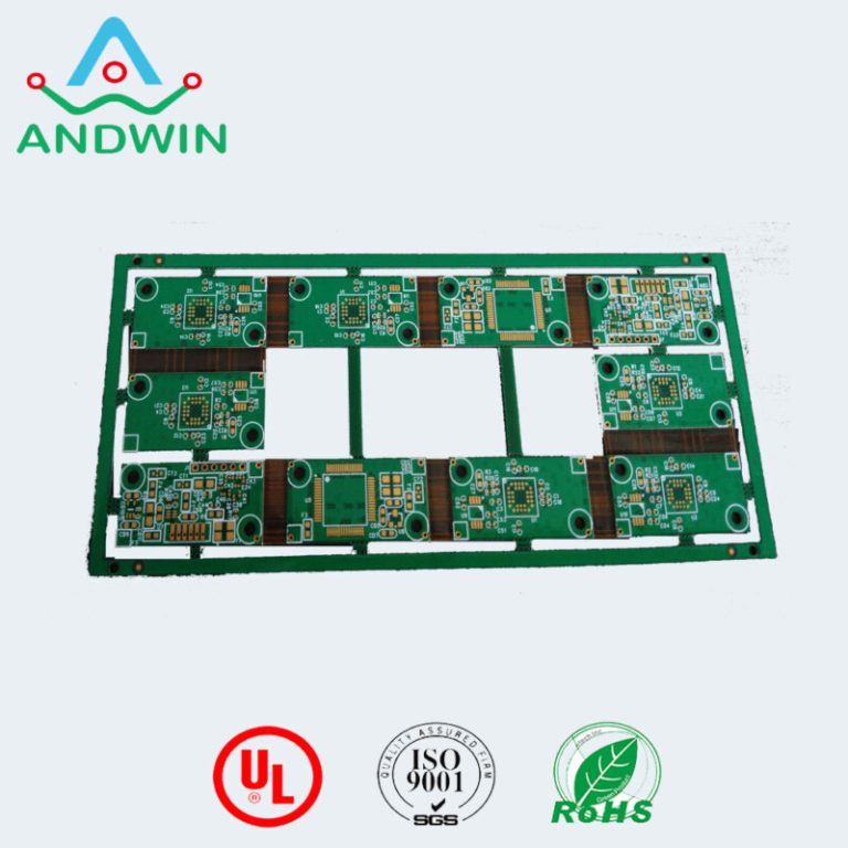
To begin with, ceramic PCBs are favored in applications where high thermal performance is required, such as in LED lighting, power electronics, and aerospace industries.
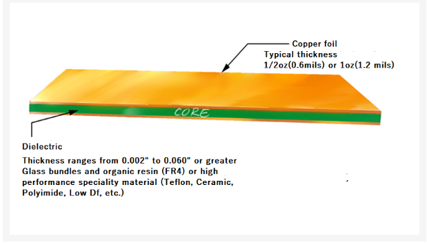
The ceramic material, often made from alumina or aluminum nitride, provides excellent thermal conductivity, allowing heat to dissipate efficiently from the electronic components. This characteristic is crucial in preventing overheating and ensuring the longevity of the device. Consequently, the reflow process for ceramic PCBs must be carefully controlled to maintain the integrity of both the substrate and the components.
The reflow process typically involves several stages, starting with the application of solder paste onto the ceramic substrate.
This paste is a mixture of solder powder and flux, which helps to clean the surfaces and improve the wetting of the solder. The components are then placed onto the substrate, aligning with the solder paste. Following this, the assembly is subjected to a controlled heating process in a reflow oven. The temperature profile of the oven is meticulously designed to ensure that the solder melts and forms a strong bond without damaging the components or the ceramic substrate.
One of the challenges in ceramic PCB reflow is managing the thermal expansion mismatch between the ceramic substrate and the electronic components.
Unlike traditional PCBs made from materials like FR-4, ceramic substrates have different thermal expansion coefficients. This discrepancy can lead to mechanical stress during the heating and cooling phases of the reflow process, potentially causing defects such as solder joint cracking or component misalignment. To mitigate these risks, manufacturers often employ specialized solder alloys and carefully controlled temperature profiles.
Moreover, the reflow process for ceramic PCBs may require different equipment and settings compared to standard PCBs.
For instance, the reflow oven must be capable of reaching higher temperatures to accommodate the melting point of the solder used with ceramic substrates. Additionally, the cooling rate must be precisely controlled to prevent thermal shock, which can lead to cracking or warping of the ceramic material. These considerations highlight the importance of expertise and precision in the reflow process for ceramic PCBs.
In conclusion, ceramic PCB reflow is a sophisticated process that demands a thorough understanding of both the materials involved and the thermal dynamics at play.
By carefully managing the reflow parameters, manufacturers can ensure the production of reliable and high-performance electronic devices. As technology continues to advance, the demand for ceramic PCBs is likely to grow, making the mastery of this process increasingly important. Through continued research and development, the industry can further refine ceramic PCB reflow techniques, paving the way for more efficient and durable electronic components.
Advantages Of Using Ceramic PCBs In Reflow Processes
Ceramic printed circuit boards (PCBs) have emerged as a significant advancement in the field of electronics manufacturing, particularly in reflow processes. The reflow process, a critical step in surface mount technology (SMT), involves the melting of solder to create electrical connections between components and the PCB. The choice of substrate material in this process is crucial, as it directly impacts the performance, reliability, and efficiency of the final product. Ceramic PCBs offer several advantages over traditional materials like FR-4, making them an attractive option for manufacturers seeking to optimize their reflow processes.
One of the primary advantages of ceramic PCBs in reflow processes is their superior thermal conductivity.
Ceramic materials, such as aluminum oxide (Al2O3) and aluminum nitride (AlN), possess excellent thermal properties that allow for efficient heat dissipation. This characteristic is particularly beneficial in high-power applications where excessive heat can lead to component failure or reduced performance. By effectively managing heat, ceramic PCBs help maintain the integrity of the solder joints during the reflow process, thereby enhancing the overall reliability of the electronic assembly.
In addition to thermal conductivity, ceramic PCBs exhibit remarkable thermal stability.
Unlike traditional substrates, ceramics can withstand higher temperatures without degrading, which is crucial during the reflow process where temperatures can reach up to 250°C. This thermal stability ensures that the ceramic substrate maintains its structural integrity, preventing warping or deformation that could compromise the alignment and connection of components. Consequently, manufacturers can achieve higher yields and reduce the risk of defects, leading to cost savings and improved product quality.
Moreover, ceramic PCBs offer excellent electrical insulation properties.
The inherent dielectric strength of ceramic materials ensures minimal electrical interference, which is essential for maintaining signal integrity in high-frequency applications. This advantage is particularly relevant in the context of reflow processes, where precise control over electrical characteristics is necessary to ensure optimal performance of the final product. By minimizing signal loss and crosstalk, ceramic PCBs contribute to the development of more efficient and reliable electronic devices.
Furthermore, the mechanical robustness of ceramic PCBs cannot be overlooked.
Ceramics are inherently rigid and resistant to mechanical stress, making them ideal for applications that require durability and longevity. During the reflow process, this mechanical strength helps prevent damage from thermal expansion and contraction, which can lead to micro-cracks or delamination in less robust materials. As a result, ceramic PCBs are well-suited for use in harsh environments where mechanical reliability is paramount.
In addition to these technical advantages, ceramic PCBs also offer environmental benefits.
Ceramics are generally more environmentally friendly than traditional PCB materials, as they do not contain harmful substances like halogens or heavy metals. This aligns with the growing demand for sustainable manufacturing practices and compliance with environmental regulations. By choosing ceramic PCBs, manufacturers can reduce their environmental footprint while still achieving high-performance outcomes.
In conclusion, the use of ceramic PCBs in reflow processes presents numerous advantages that enhance the performance, reliability, and sustainability of electronic assemblies.
Their superior thermal conductivity, thermal stability, electrical insulation, mechanical robustness, and environmental benefits make them an ideal choice for manufacturers seeking to optimize their production processes. As the demand for high-performance electronic devices continues to grow, the adoption of ceramic PCBs in reflow processes is likely to become increasingly prevalent, driving innovation and efficiency in the electronics industry.
Key Challenges In Ceramic PCB Reflow And How To Overcome Them
Ceramic printed circuit boards (PCBs) have become increasingly popular in various high-performance applications due to their superior thermal conductivity, mechanical strength, and electrical insulation properties.
However, the reflow process for ceramic PCBs presents unique challenges that must be addressed to ensure optimal performance and reliability. Understanding these challenges and implementing effective strategies to overcome them is crucial for manufacturers aiming to leverage the benefits of ceramic PCBs.
One of the primary challenges in ceramic PCB reflow is the material’s inherent thermal properties.
Unlike traditional FR-4 substrates, ceramic materials such as alumina and aluminum nitride have high thermal conductivity, which can lead to rapid heat dissipation during the reflow process.
This characteristic necessitates precise control of the reflow oven’s temperature profile to ensure that the solder paste reaches the appropriate melting point without causing thermal shock to the components. To address this, manufacturers can employ advanced reflow ovens equipped with multiple heating zones and precise temperature control systems. These ovens allow for gradual heating and cooling, minimizing the risk of thermal stress and ensuring uniform solder joint formation.
Another significant challenge is the potential for warping or cracking of the ceramic substrate during the reflow process.
Ceramic materials, while robust, can be brittle and susceptible to mechanical stress. The mismatch in thermal expansion coefficients between the ceramic substrate and the components can exacerbate this issue, leading to mechanical failures.
To mitigate this risk, manufacturers can use specialized solder pastes designed for ceramic applications. These solder pastes often contain additives that enhance their flexibility and reduce the likelihood of mechanical stress during thermal cycling. Additionally, implementing a carefully controlled cooling process can help prevent rapid temperature changes that contribute to substrate warping or cracking.
The reflow process for ceramic PCBs also demands meticulous attention to the selection of compatible components and materials.
The high reflow temperatures required for ceramic substrates can exceed the tolerance levels of standard electronic components, leading to potential damage or failure. Therefore, it is essential to select components that can withstand the elevated temperatures associated with ceramic PCB reflow.
Manufacturers can collaborate with component suppliers to identify suitable materials and components that are specifically designed for high-temperature applications. This collaboration ensures that all elements of the assembly are compatible and capable of enduring the reflow process without compromising performance.
Furthermore, achieving consistent solder joint quality is a critical aspect of ceramic PCB reflow.
The high thermal conductivity of ceramic substrates can lead to uneven heat distribution, resulting in incomplete solder reflow or void formation.
To overcome this challenge, manufacturers can employ advanced inspection techniques such as X-ray imaging and automated optical inspection (AOI) to detect and address solder joint defects.
These technologies enable real-time monitoring and quality control, allowing for immediate adjustments to the reflow process if necessary.
In conclusion, while the reflow process for ceramic PCBs presents several challenges, these can be effectively managed through careful planning and the implementation of advanced technologies.
By understanding the unique thermal and mechanical properties of ceramic materials, manufacturers can optimize the reflow process to ensure reliable and high-performance ceramic PCB assemblies. Through precise temperature control, the use of specialized materials, and rigorous quality inspection, the challenges associated with ceramic PCB reflow can be successfully overcome, paving the way for their broader adoption in demanding applications.
Innovations In Ceramic PCB Reflow Technology
Ceramic printed circuit boards (PCBs) have become increasingly significant in the electronics industry due to their superior thermal conductivity, mechanical strength, and electrical insulation properties. As the demand for high-performance electronic devices continues to rise, innovations in ceramic PCB reflow technology have emerged as a critical area of focus.
These advancements aim to enhance the efficiency, reliability, and quality of the reflow process, which is essential for the successful assembly of electronic components onto ceramic substrates.
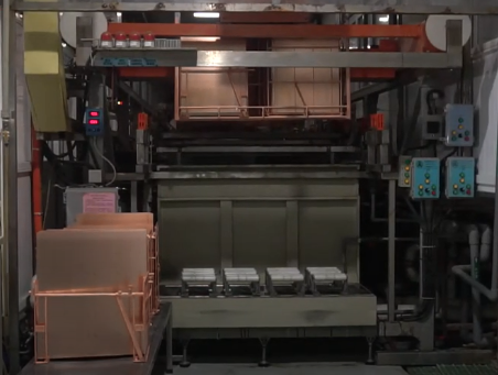
One of the primary innovations in ceramic PCB reflow technology is the development of advanced reflow ovens.
These ovens are designed to provide precise temperature control and uniform heat distribution, which are crucial for achieving optimal soldering results.
By utilizing sophisticated heating elements and sensors, modern reflow ovens can maintain consistent thermal profiles, thereby minimizing the risk of thermal shock and ensuring the integrity of the ceramic material.
Furthermore, the integration of real-time monitoring systems allows for the continuous assessment of the reflow process, enabling immediate adjustments to be made if necessary.
In addition to improvements in reflow ovens, the introduction of novel solder pastes has significantly contributed to advancements in ceramic PCB reflow technology.
These solder pastes are formulated to accommodate the unique properties of ceramic substrates, such as their high thermal conductivity and low coefficient of thermal expansion. By optimizing the composition of solder pastes, manufacturers can achieve better wetting and adhesion, which are essential for forming strong and reliable solder joints. Moreover, the use of lead-free solder pastes aligns with global environmental regulations, promoting sustainability in the electronics industry.
Another noteworthy innovation is the implementation of advanced reflow profiling techniques.
Reflow profiling involves the careful analysis and optimization of the thermal profile used during the reflow process. By employing sophisticated software tools and thermal imaging technologies, engineers can develop customized reflow profiles that cater to the specific requirements of ceramic PCBs.
This tailored approach not only enhances the quality of solder joints but also reduces the likelihood of defects such as voids and tombstoning, which can compromise the performance of electronic devices.
Furthermore, the adoption of vacuum reflow technology has emerged as a game-changer in the realm of ceramic PCB reflow.
Vacuum reflow involves the application of a vacuum environment during the reflow process, which effectively eliminates air pockets and reduces the occurrence of voids in solder joints. This technique is particularly beneficial for ceramic PCBs, as it enhances the thermal and mechanical reliability of the assembled components. By ensuring a void-free soldering process, vacuum reflow technology contributes to the overall durability and longevity of electronic devices.
In conclusion, the continuous innovations in ceramic PCB reflow technology are pivotal in meeting the evolving demands of the electronics industry.
Through advancements in reflow ovens, solder paste formulations, reflow profiling techniques, and vacuum reflow technology, manufacturers can achieve higher levels of precision, reliability, and efficiency in the assembly of ceramic PCBs. As these technologies continue to evolve, they hold the potential to further revolutionize the production of high-performance electronic devices, paving the way for future innovations in the field.
Best Practices For Successful Ceramic PCB Reflow
Ceramic printed circuit boards (PCBs) have become increasingly popular in various high-performance applications due to their superior thermal conductivity, mechanical strength, and electrical insulation properties.
As the demand for these advanced materials grows, understanding the best practices for successful ceramic PCB reflow becomes essential for manufacturers aiming to achieve optimal performance and reliability.
The reflow process, a critical step in the assembly of PCBs, involves the controlled heating of solder paste to create reliable electrical connections between components and the board. However, the unique properties of ceramic substrates necessitate specific considerations to ensure a successful outcome.
To begin with, selecting the appropriate solder paste is crucial.
Ceramic PCBs often require solder pastes with higher melting points compared to those used with traditional FR-4 substrates. This is due to the ceramic material’s ability to withstand higher temperatures without degradation.
Therefore, manufacturers should opt for solder pastes specifically formulated for high-temperature applications, ensuring compatibility with the ceramic substrate and the components being used.
Additionally, the choice of flux within the solder paste can significantly impact the reflow process. A flux that provides excellent wetting properties and leaves minimal residue is ideal, as it enhances the solder joint quality and reduces the need for post-reflow cleaning.
Moreover, the reflow profile must be carefully tailored to accommodate the thermal characteristics of ceramic PCBs.
Unlike traditional PCBs, ceramic substrates exhibit different thermal expansion coefficients, which can lead to stress and potential damage if not properly managed. A well-designed reflow profile should include a gradual ramp-up in temperature to minimize thermal shock, followed by a controlled soak period to ensure uniform heat distribution across the board. The peak temperature should be high enough to adequately melt the solder paste but not so high as to risk damaging the components or the substrate. Finally, a gradual cooling phase is essential to prevent thermal stress and ensure the integrity of the solder joints.
In addition to temperature considerations, the atmosphere within the reflow oven plays a significant role in the success of the process.
An inert atmosphere, typically achieved by introducing nitrogen, can help prevent oxidation of the solder and components, leading to higher quality solder joints. This is particularly important for ceramic PCBs, as the high reflow temperatures can exacerbate oxidation issues. Maintaining a controlled atmosphere throughout the reflow process can significantly enhance the reliability and performance of the final product.
Furthermore, attention to detail in the placement of components is vital.
The precision of component placement directly affects the quality of the solder joints and the overall functionality of the PCB. Automated pick-and-place machines should be calibrated to ensure accurate positioning, and any misalignment should be corrected before reflow. This step is crucial in preventing defects such as tombstoning or bridging, which can compromise the electrical performance of the board.
Finally, post-reflow inspection and testing are indispensable in verifying the success of the reflow process.
Advanced inspection techniques, such as X-ray and automated optical inspection (AOI), can detect defects that are not visible to the naked eye, ensuring that any issues are identified and rectified before the PCB is deployed. By adhering to these best practices, manufacturers can achieve successful ceramic PCB reflow, resulting in high-quality, reliable products that meet the demanding requirements of modern electronic applications.