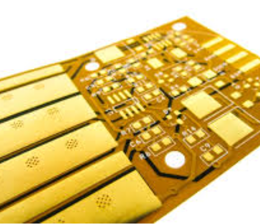
Ceramic pcb thick film
Advantages Of Ceramic PCB Thick Film Technology
Ceramic PCB thick film technology has emerged as a pivotal advancement in the field of electronic circuit design, offering a multitude of advantages that cater to the evolving demands of modern electronics. This technology, which involves the deposition of thick film materials onto ceramic substrates, is renowned for its ability to enhance the performance and reliability of electronic devices.
One of the primary advantages of ceramic PCB thick film technology is its exceptional thermal management capabilities.
Ceramic substrates, such as alumina or aluminum nitride, possess excellent thermal conductivity, which allows for efficient heat dissipation. This is particularly beneficial in high-power applications where excessive heat can lead to device failure. By effectively managing heat, ceramic PCBs ensure the longevity and stability of electronic components, making them ideal for use in power electronics, LED lighting, and automotive applications.
In addition to superior thermal management, ceramic PCB thick film technology offers remarkable electrical insulation properties.
The inherent dielectric strength of ceramic materials provides robust insulation, which is crucial for preventing electrical breakdown and ensuring the safe operation of electronic circuits. This characteristic is especially important in high-voltage applications, where maintaining electrical integrity is paramount. Furthermore, the thick film process allows for the precise deposition of conductive, resistive, and dielectric layers, enabling the creation of complex circuit patterns with high precision and repeatability. This precision is essential for the miniaturization of electronic devices, as it allows for the integration of multiple functions within a compact footprint.
Another significant advantage of ceramic PCB thick film technology is its excellent chemical and environmental resistance.
Ceramic substrates are inherently resistant to moisture, chemicals, and other environmental factors that can degrade traditional PCB materials. This resistance ensures that electronic devices can operate reliably in harsh environments, such as those encountered in aerospace, military, and industrial applications. Moreover, the durability of ceramic PCBs reduces the need for protective coatings, which can add weight and complexity to electronic assemblies.
The mechanical robustness of ceramic PCBs is yet another noteworthy benefit.
Ceramic materials are known for their high mechanical strength and rigidity, which provide structural support to electronic components and protect them from mechanical stress and vibration. This robustness is particularly advantageous in applications where mechanical stability is critical, such as in automotive and aerospace systems. Additionally, the dimensional stability of ceramic substrates ensures that circuit patterns remain accurate and reliable over time, even under varying temperature and humidity conditions.
Furthermore, ceramic PCB thick film technology is highly versatile, accommodating a wide range of materials and processes to meet specific application requirements.
This versatility allows for the customization of circuit designs to achieve optimal performance characteristics, such as tailored resistance values or specific thermal properties. The ability to fine-tune these parameters makes ceramic PCBs suitable for a diverse array of applications, from consumer electronics to advanced medical devices.
In conclusion, ceramic PCB thick film technology offers a host of advantages that make it an attractive choice for modern electronic applications. Its superior thermal management, electrical insulation, chemical resistance, mechanical robustness, and versatility collectively contribute to the enhanced performance and reliability of electronic devices. As the demand for high-performance, durable, and miniaturized electronic solutions continues to grow, ceramic PCB thick film technology is poised to play an increasingly important role in meeting these challenges.
Applications Of Thick Film Ceramic PCBs In Modern Electronics
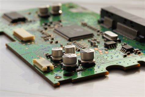
Thick film ceramic PCBs have emerged as a pivotal component in the landscape of modern electronics, offering a unique blend of durability, thermal management, and miniaturization. These attributes make them indispensable in a variety of applications, ranging from consumer electronics to industrial and automotive sectors. As the demand for more efficient and compact electronic devices continues to rise, the role of thick film ceramic PCBs becomes increasingly significant.
One of the primary applications of thick film ceramic PCBs is in the realm of high-frequency communication devices.
The inherent properties of ceramic materials, such as low dielectric loss and high thermal conductivity, make them ideal for use in RF and microwave circuits. These characteristics ensure minimal signal loss and effective heat dissipation, which are crucial for maintaining the performance and reliability of communication devices. Consequently, thick film ceramic PCBs are extensively used in satellite communication systems, radar technology, and mobile communication infrastructure.
In addition to communication devices, thick film ceramic PCBs are also widely utilized in the automotive industry.
The automotive sector demands components that can withstand harsh environmental conditions, including extreme temperatures and vibrations. Thick film ceramic PCBs meet these requirements due to their robust nature and excellent thermal stability. They are commonly found in engine control units, transmission control systems, and various sensors that are integral to modern vehicles. As the automotive industry shifts towards electric and autonomous vehicles, the need for reliable and efficient electronic components is more critical than ever, further cementing the importance of thick film ceramic PCBs.
Moreover, the medical electronics field benefits significantly from the use of thick film ceramic PCBs.
Medical devices often require high precision and reliability, as they are used in life-critical applications. The biocompatibility and stability of ceramic materials make them suitable for use in implantable devices, diagnostic equipment, and patient monitoring systems. Thick film ceramic PCBs provide the necessary performance and reliability, ensuring that medical devices function accurately and consistently over extended periods.
Furthermore, the industrial sector leverages thick film ceramic PCBs for their ability to operate in demanding environments.
Industrial applications often involve exposure to high temperatures, corrosive substances, and mechanical stress. Thick film ceramic PCBs are employed in power electronics, motor drives, and industrial automation systems, where their durability and thermal management capabilities are essential. These PCBs contribute to the efficiency and longevity of industrial equipment, reducing downtime and maintenance costs.
In the realm of consumer electronics, the trend towards miniaturization and enhanced functionality drives the adoption of thick film ceramic PCBs.
Devices such as smartphones, tablets, and wearable technology require compact and efficient circuit boards to accommodate their complex functionalities. The high-density interconnects and superior thermal properties of thick film ceramic PCBs enable the development of smaller, more powerful consumer electronics, meeting the ever-evolving demands of the market.
In conclusion, thick film ceramic PCBs play a crucial role in modern electronics across various industries. Their unique properties, including excellent thermal management, durability, and miniaturization capabilities, make them suitable for a wide range of applications. As technology continues to advance, the demand for these versatile components is expected to grow, underscoring their importance in the future of electronic device development.

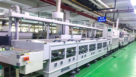
Manufacturing Process Of Ceramic PCB Thick Film
The manufacturing process of ceramic PCB thick film is a sophisticated and intricate procedure that plays a crucial role in the production of high-performance electronic components. This process begins with the selection of a suitable ceramic substrate, which serves as the foundation for the thick film circuitry. Typically, materials such as alumina, aluminum nitride, or beryllium oxide are chosen for their excellent thermal conductivity, electrical insulation properties, and mechanical strength. These substrates are meticulously prepared to ensure a smooth and clean surface, which is essential for the subsequent application of thick film materials.
Once the substrate is prepared, the next step involves the application of thick film pastes.
These pastes are composed of a mixture of conductive, resistive, or dielectric materials suspended in an organic binder. The choice of paste depends on the specific electrical properties required for the circuit. The application of these pastes is typically carried out using screen printing techniques, which allow for precise deposition of the material onto the substrate. Screen printing involves the use of a mesh stencil to transfer the paste onto the substrate in the desired pattern, ensuring accuracy and repeatability in the circuit design.
Following the application of the thick film pastes, the printed substrates undergo a drying process to remove the organic solvents present in the paste.
This step is crucial to prevent any defects or inconsistencies in the final product. The drying process is typically conducted in a controlled environment to ensure uniformity and to prepare the substrate for the subsequent firing stage. Firing, also known as sintering, is a critical step in the manufacturing process, as it transforms the printed pastes into solid, functional films. This is achieved by subjecting the substrates to high temperatures in a furnace, which causes the organic binders to burn off and the inorganic particles to fuse together, forming a dense and adherent film.
The firing process must be carefully controlled to achieve the desired electrical and mechanical properties of the thick film.
Factors such as temperature, time, and atmosphere within the furnace are meticulously monitored to ensure optimal results. Once the firing process is complete, the substrates are allowed to cool gradually to prevent thermal shock and potential damage to the films. At this stage, the ceramic PCB thick film is nearly complete, but additional steps may be required to enhance its performance or to meet specific design requirements.
These additional steps may include the application of protective coatings, laser trimming to adjust resistor values, or the addition of solderable surfaces for component attachment.
Each of these processes is carried out with precision to maintain the integrity and functionality of the thick film circuit. Finally, the completed ceramic PCB thick film undergoes rigorous testing and inspection to ensure it meets the required specifications and quality standards. This includes electrical testing to verify circuit functionality and visual inspection to detect any defects or irregularities.
In conclusion, the manufacturing process of ceramic PCB thick film is a complex and highly controlled procedure that demands precision and expertise. From substrate preparation to the final testing phase, each step is critical in producing reliable and high-performance electronic components. The use of ceramic materials and thick film technology offers significant advantages in terms of thermal management, electrical performance, and durability, making it an essential process in the electronics industry.
Comparing Thick Film And Thin Film Ceramic PCBs
Ceramic printed circuit boards (PCBs) have become increasingly popular in various high-performance applications due to their superior thermal and electrical properties. Among the different types of ceramic PCBs, thick film and thin film technologies stand out as the most prevalent. Understanding the distinctions between these two technologies is crucial for selecting the appropriate solution for specific applications.
Thick film ceramic PCBs are characterized by the deposition of conductive, resistive, and dielectric pastes onto a ceramic substrate.
This process involves screen printing multiple layers of these pastes, which are then fired at high temperatures to form a solid, durable film. One of the primary advantages of thick film technology is its robustness. The resulting circuits are highly resistant to environmental factors such as temperature fluctuations, humidity, and chemical exposure. This makes thick film ceramic PCBs ideal for harsh environments, including automotive and industrial applications.
In contrast, thin film ceramic PCBs are produced using a different approach.
This technology involves the deposition of a very thin layer of conductive material onto the ceramic substrate, typically through sputtering or evaporation techniques. The thin film process allows for the creation of highly precise and intricate circuit patterns, which is a significant advantage in applications requiring miniaturization and high-density interconnections. Consequently, thin film ceramic PCBs are often favored in the medical and aerospace industries, where precision and reliability are paramount.
While both thick film and thin film ceramic PCBs offer distinct benefits, they also present unique challenges.
Thick film PCBs, for instance, may have limitations in terms of achieving very fine line widths and spaces due to the nature of the screen printing process. This can be a drawback in applications where miniaturization is critical. However, the ability to deposit multiple layers of materials allows for the integration of various passive components directly onto the substrate, which can be advantageous in simplifying circuit design and reducing overall system size.
On the other hand, thin film ceramic PCBs excel in applications requiring high precision and fine feature sizes.
The thin film process enables the creation of extremely fine lines and spaces, which is essential for high-frequency applications and complex circuit designs. However, the production of thin film PCBs can be more costly and time-consuming compared to thick film technology, primarily due to the sophisticated equipment and processes involved.
In terms of thermal management, both thick film and thin film ceramic PCBs offer excellent performance due to the inherent properties of the ceramic substrate.
Ceramic materials provide superior heat dissipation compared to traditional FR-4 substrates, making them suitable for high-power applications. However, the choice between thick film and thin film may depend on the specific thermal requirements of the application, as well as other factors such as cost and design complexity.
In conclusion, the decision between thick film and thin film ceramic PCBs should be guided by the specific needs of the application. Thick film technology offers durability and environmental resistance, making it suitable for rugged applications, while thin film technology provides precision and miniaturization capabilities, ideal for high-density and high-frequency applications. By carefully considering the advantages and limitations of each technology, designers can select the most appropriate ceramic PCB solution to meet their performance and reliability requirements.