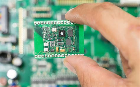
Ceramic PCBs: A Comprehensive Guide to Design, Manufacturing, and Applications
Ceramic Printed Circuit Boards (PCBs) are a specialized type of PCB that offer superior thermal, electrical, and mechanical properties compared to traditional FR-4 or metal-core PCBs. Made from ceramic materials such as aluminum oxide (Al₂O₃), aluminum nitride (AlN), or beryllium oxide (BeO), ceramic PCBs are ideal for high-performance applications where reliability, thermal management, and miniaturization are critical. This article provides a comprehensive guide to ceramic PCBs, covering their materials, manufacturing processes, design considerations, advantages, disadvantages, and applications.
1. Introduction to Ceramic PCBs
Ceramic PCBs are constructed using ceramic substrates instead of the traditional epoxy-based laminates used in FR-4 PCBs. These substrates are composed of inorganic materials, such as alumina, aluminum nitride, or beryllium oxide, which provide exceptional thermal conductivity, electrical insulation, and mechanical stability. Ceramic PCBs are widely used in high-power, high-frequency, and high-temperature applications, including aerospace, automotive, telecommunications, and medical devices.
2. Materials Used in Ceramic PCBs
The choice of ceramic material significantly impacts the performance and suitability of the PCB for specific applications. The most commonly used ceramic materials are:
2.1 Aluminum Oxide (Al₂O₃)
Alumina is the most widely used ceramic material for PCBs due to its excellent balance of properties and cost-effectiveness.
- Thermal Conductivity: 24-28 W/mK.
- Electrical Insulation: High dielectric strength.
- Mechanical Strength: Good mechanical stability and hardness.
- Applications: LED lighting, power electronics, and automotive systems.
2.2 Aluminum Nitride (AlN)
Aluminum nitride offers superior thermal conductivity compared to alumina, making it ideal for high-power applications.
- Thermal Conductivity: 140-180 W/mK.
- Electrical Insulation: Excellent dielectric properties.
- Mechanical Strength: Lower than alumina but sufficient for most applications.
- Applications: High-power LEDs, RF/microwave circuits, and semiconductor packaging.
2.3 Beryllium Oxide (BeO)
Beryllium oxide has the highest thermal conductivity among ceramic materials but is less commonly used due to its toxicity.
- Thermal Conductivity: 250-300 W/mK.
- Electrical Insulation: Excellent dielectric properties.
- Mechanical Strength: Moderate.
- Applications: High-power RF devices, aerospace systems, and military electronics.
3. Manufacturing Processes for Ceramic PCBs
The manufacturing of ceramic PCBs involves specialized processes to ensure the desired electrical, thermal, and mechanical properties. Key manufacturing steps include:
3.1 Substrate Preparation
The ceramic substrate is prepared by mixing raw ceramic powders with binders and sintering aids. The mixture is then pressed into sheets and sintered at high temperatures to form a dense, solid substrate.
3.2 Metallization
Metallization involves depositing conductive traces onto the ceramic substrate. Common metallization techniques include:
- Thick-Film Printing: Conductive pastes (e.g., silver, gold, or copper) are screen-printed onto the substrate and fired at high temperatures.
- Thin-Film Deposition: Conductive layers are deposited using techniques such as sputtering or evaporation, followed by photolithography to define the circuit pattern.
- Direct Bonded Copper (DBC): A copper foil is bonded to the ceramic substrate at high temperatures, providing excellent thermal and electrical conductivity.
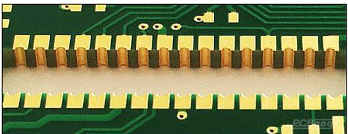
3.3 Via Formation
Vias are created in ceramic PCBs using laser drilling or mechanical drilling. The vias are then filled with conductive material to establish electrical connections between layers.
3.4 Surface Finishing
A surface finish, such as electroless nickel immersion gold (ENIG) or immersion silver, is applied to protect the conductive traces and enhance solderability.
3.5 Assembly and Testing
Components are assembled onto the ceramic PCB using soldering or wire bonding. The finished PCB undergoes rigorous testing to ensure electrical performance, thermal management, and reliability.
4. Design Considerations for Ceramic PCB
Designing ceramic PCBs requires careful consideration of their unique properties and manufacturing constraints. Key design considerations include:
4.1 Thermal Management
Ceramic PCBs are often used in high-power applications where heat dissipation is critical. Designers should:
- Maximize the use of thermal vias to transfer heat to the substrate.
- Optimize the layout to minimize thermal resistance.
- Integrate heat sinks or cooling systems for additional thermal management.
4.2 Electrical Performance
Ceramic materials have excellent dielectric properties, making them suitable for high-frequency and high-speed applications. Designers should:
- Minimize trace lengths to reduce signal loss and impedance mismatches.
- Use controlled impedance routing for high-frequency signals.
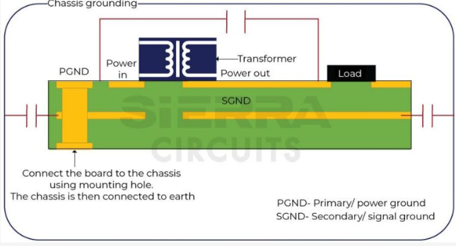
- Ensure proper grounding to minimize electromagnetic interference (EMI).
4.3 Mechanical Stability
Ceramic PCBs are brittle and prone to cracking under mechanical stress. Designers should:
- Avoid sharp corners and stress concentrators in the layout.
- Use appropriate mounting techniques to minimize mechanical stress.
- Consider the coefficient of thermal expansion (CTE) mismatch between the ceramic substrate and components.
4.4 Miniaturization
Ceramic PCBs are ideal for miniaturized designs due to their high density and precision. Designers should:
- Use fine-pitch components and high-density interconnects (HDI).
- Optimize the layout to maximize space utilization.
- Leverage advanced manufacturing techniques, such as laser drilling and thin-film deposition.
5. Advantages of Ceramic PCBs
5.1 Superior Thermal Conductivity
Ceramic materials have much higher thermal conductivity than FR-4 or metal-core PCBs, enabling efficient heat dissipation in high-power applications.
5.2 Excellent Electrical Insulation
Ceramic substrates provide high dielectric strength and low dielectric loss, making them ideal for high-frequency and high-voltage applications.
5.3 High Mechanical Stability
Ceramic PCBs are resistant to wear, corrosion, and thermal shock, ensuring long-term reliability in harsh environments.
5.4 Miniaturization
The high density and precision of ceramic PCBs enable the design of compact, lightweight electronic systems.
6. Disadvantages of Ceramic PCBs
6.1 High Cost
Ceramic PCBs are more expensive than traditional PCBs due to the cost of materials and specialized manufacturing processes.
6.2 Brittleness
Ceramic materials are brittle and prone to cracking under mechanical stress, requiring careful handling and mounting.
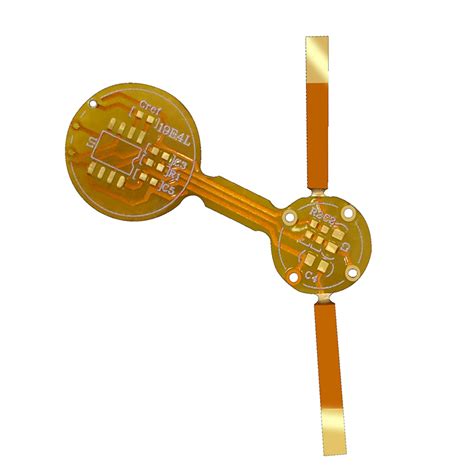
6.3 Limited Flexibility
Ceramic PCBs are rigid and cannot be used in flexible or bendable applications.
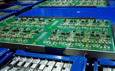
7. Applications of Ceramic PCBs
7.1 LED Lighting
Ceramic PCBs are widely used in high-power LED lighting due to their excellent thermal management and reliability.
7.2 Power Electronics
Ceramic PCBs are ideal for power electronics, such as inverters, converters, and motor drives, where high thermal conductivity and electrical insulation are required.
7.3 RF and Microwave Circuits
The low dielectric loss and high-frequency performance of ceramic PCBs make them suitable for RF and microwave applications, such as antennas and amplifiers.
7.4 Aerospace and Defense
Ceramic PCBs are used in aerospace and defense systems due to their ability to withstand extreme temperatures, vibrations, and radiation.
7.5 Medical Devices
Ceramic PCBs are used in medical devices, such as imaging systems and implantable devices, where reliability and miniaturization are critical.
8. Emerging Trends in Ceramic PCBs
8.1 Advanced Materials
Research is ongoing to develop new ceramic materials with enhanced properties, such as higher thermal conductivity and improved mechanical strength.
8.2 Additive Manufacturing
Additive manufacturing techniques, such as 3D printing, are being explored to create complex ceramic PCB structures with reduced waste and cost.
8.3 Integration with Other Technologies
Ceramic PCBs are being integrated with other advanced technologies, such as embedded components and flexible circuits, to create hybrid solutions for next-generation electronics.
9. Conclusion
Ceramic PCBs offer unparalleled thermal, electrical, and mechanical properties, making them ideal for high-performance applications in industries such as aerospace, automotive, telecommunications, and medical devices. While they come with challenges, such as high cost and brittleness, their advantages often outweigh the drawbacks in demanding environments. By understanding the materials, manufacturing processes, and design considerations associated with ceramic PCBs, engineers can leverage their unique capabilities to create innovative and reliable electronic systems. Emerging trends, such as advanced materials and additive manufacturing, are poised to further expand the possibilities of ceramic PCBs, driving advancements in technology and industry.