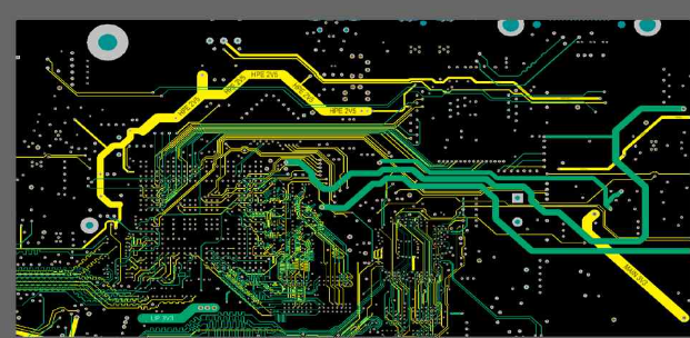
Ceramic rf pcb
Advantages Of Ceramic RF PCB In High-Frequency Applications
Ceramic RF PCBs, or radio frequency printed circuit boards, have emerged as a pivotal component in high-frequency applications, offering a range of advantages that make them indispensable in modern technology.
As the demand for faster and more reliable communication systems continues to grow, the need for materials that can support high-frequency signals without significant loss or interference becomes increasingly critical. Ceramic materials, known for their excellent electrical properties, provide a robust solution for these challenges.
One of the primary advantages of ceramic RF PCBs is their superior thermal performance.
Unlike traditional materials such as FR-4, ceramics can withstand higher temperatures without degrading. This thermal stability is crucial in high-frequency applications where components often generate significant heat. The ability of ceramic materials to dissipate heat efficiently ensures that the performance of the RF circuits remains consistent, thereby enhancing the reliability and longevity of the devices in which they are used. Furthermore, this thermal resilience reduces the risk of thermal expansion, which can lead to mechanical stress and potential failure in other types of PCBs.
In addition to thermal advantages, ceramic RF PCBs offer exceptional electrical properties.
The dielectric constant of ceramic materials is typically higher than that of conventional PCB substrates, which allows for the miniaturization of components without compromising performance. This is particularly beneficial in applications where space is at a premium, such as in mobile devices and aerospace technologies. Moreover, the low dielectric loss of ceramics ensures that signal integrity is maintained even at high frequencies, minimizing the risk of signal distortion and ensuring clear and accurate data transmission.
Another significant benefit of ceramic RF PCBs is their mechanical strength and durability.
Ceramics are inherently robust and resistant to environmental factors such as moisture, chemicals, and mechanical wear. This makes them ideal for use in harsh environments where other materials might fail. The mechanical stability of ceramic PCBs also contributes to their ability to maintain precise electrical characteristics over time, which is essential for applications that require long-term reliability.
Furthermore, ceramic RF PCBs are highly customizable, allowing for the integration of various components and the creation of complex circuit designs.
This flexibility is particularly advantageous in the development of advanced communication systems, where specific design requirements must be met to achieve optimal performance. The ability to tailor the properties of ceramic materials to suit specific applications enables engineers to push the boundaries of what is possible in high-frequency technology.
In conclusion, the advantages of ceramic RF PCBs in high-frequency applications are manifold.
3 Their superior thermal performance, exceptional electrical properties, mechanical strength, and customization capabilities make them an ideal choice for a wide range of advanced technologies. As the demand for high-frequency applications continues to rise, the role of ceramic RF PCBs is likely to become even more prominent, driving innovation and enabling the development of faster, more reliable communication systems. By leveraging the unique properties of ceramic materials, engineers can design and implement solutions that meet the ever-evolving needs of modern technology, ensuring that communication systems remain at the forefront of performance and reliability.
Design Considerations For Ceramic RF PCB
When designing ceramic RF PCBs, several critical considerations must be taken into account to ensure optimal performance and reliability. Ceramic substrates are increasingly favored in RF applications due to their superior thermal properties, high-frequency performance, and mechanical stability. However, the unique characteristics of ceramic materials necessitate a distinct approach to design compared to traditional FR-4 substrates.
To begin with, the choice of ceramic material is paramount. Commonly used ceramics in RF PCBs include alumina, aluminum nitride, and beryllium oxide, each offering different thermal conductivities and dielectric constants.
Alumina, for instance, is widely used due to its cost-effectiveness and adequate thermal performance, while aluminum nitride is preferred for applications requiring higher thermal conductivity. The dielectric constant of the ceramic material directly influences the impedance and signal integrity of the RF circuit, making it crucial to select a material that aligns with the specific frequency requirements of the application.
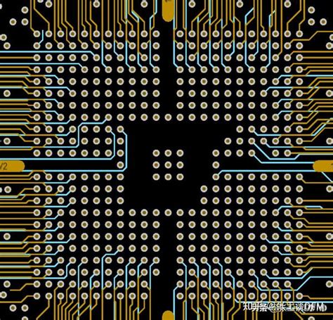
Transitioning to the layout design, the precision in the patterning of the conductive traces is critical.
Ceramic substrates allow for fine line definition, which is essential for high-frequency applications where signal integrity is paramount. The trace width and spacing must be meticulously calculated to minimize losses and crosstalk. Additionally, the use of via structures in ceramic RF PCBs requires careful consideration. Unlike traditional PCBs, vias in ceramic substrates are often filled with conductive materials to maintain electrical continuity and thermal performance. The placement and size of these vias can significantly impact the overall performance of the PCB, necessitating precise engineering.
Furthermore, thermal management is a significant concern in the design of ceramic RF PCBs.
The high thermal conductivity of ceramic materials aids in dissipating heat generated by high-power RF components. However, the design must incorporate adequate thermal vias and heat sinks to effectively manage heat distribution across the board. This is particularly important in applications such as power amplifiers and transmitters, where excessive heat can lead to performance degradation or failure.
In addition to thermal considerations, mechanical stability is another advantage of ceramic substrates.
Their inherent rigidity and resistance to environmental factors such as moisture and temperature fluctuations make them ideal for harsh environments. However, this rigidity also means that ceramic PCBs are more brittle than their FR-4 counterparts, necessitating careful handling and mounting to prevent mechanical damage.
Moreover, the integration of passive components directly onto the ceramic substrate is a design consideration that can enhance performance.
Ceramic substrates allow for the embedding of capacitors, inductors, and resistors, reducing parasitic effects and improving the overall performance of the RF circuit. This integration can also lead to a reduction in the size and weight of the final product, which is advantageous in applications where space and weight are critical constraints.
In conclusion, the design of ceramic RF PCBs requires a comprehensive understanding of the material properties and their impact on electrical, thermal, and mechanical performance. By carefully selecting the appropriate ceramic material, optimizing the layout for high-frequency operation, and addressing thermal and mechanical challenges, designers can leverage the benefits of ceramic substrates to achieve superior performance in RF applications. As technology continues to advance, the role of ceramic RF PCBs in enabling high-frequency, high-power applications is likely to expand, underscoring the importance of meticulous design considerations.
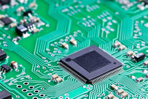
Manufacturing Process Of Ceramic RF PCB
The manufacturing process of ceramic RF PCBs, or radio frequency printed circuit boards, is a sophisticated and intricate procedure that demands precision and expertise. These PCBs are integral to high-frequency applications, where performance and reliability are paramount. The journey begins with the selection of the appropriate ceramic material, which is crucial due to its dielectric properties, thermal stability, and mechanical strength. Commonly used materials include alumina, aluminum nitride, and beryllium oxide, each offering distinct advantages depending on the specific application requirements.
Once the material is selected, the next step involves the preparation of the ceramic substrate.
This process typically includes cutting the ceramic into the desired size and shape, followed by a thorough cleaning to remove any contaminants that could affect the subsequent steps. The substrate is then subjected to a surface treatment to enhance its adhesion properties, ensuring that the conductive layers adhere properly during the later stages of manufacturing.
Following the preparation of the substrate, the focus shifts to the application of the conductive layers.
This is achieved through a process known as screen printing, where a conductive paste, often composed of silver, gold, or copper, is applied to the ceramic surface. The paste is carefully deposited in a pattern that corresponds to the circuit design, ensuring precise alignment and connectivity. After the application of the conductive paste, the substrate undergoes a drying process to remove any solvents and prepare it for the next stage.
Subsequently, the substrate is subjected to a firing process in a high-temperature furnace.
This step is critical as it sinters the conductive paste, transforming it into a solid metal layer that is firmly bonded to the ceramic substrate. The firing process not only solidifies the conductive paths but also enhances the overall mechanical and thermal properties of the PCB. It is essential to control the temperature and duration of the firing process meticulously to prevent any defects or inconsistencies in the final product.
Once the firing process is complete, the ceramic RF PCB undergoes a series of inspections and tests to ensure its quality and performance.
These tests typically include electrical testing to verify the integrity of the conductive paths and ensure that the PCB meets the required specifications. Additionally, visual inspections are conducted to identify any surface defects or irregularities that could compromise the functionality of the PCB.
After passing the quality control checks, the ceramic RF PCB is ready for the final assembly and packaging.
This stage involves the integration of additional components, such as connectors and protective coatings, to enhance the durability and functionality of the PCB. The final product is then packaged and prepared for shipment to customers, who rely on these high-performance PCBs for a wide range of applications, including telecommunications, aerospace, and medical devices.
In conclusion, the manufacturing process of ceramic RF PCBs is a complex and meticulous procedure that requires a deep understanding of materials science and engineering principles. From the selection of the ceramic substrate to the final assembly and testing, each step is critical to ensuring the performance and reliability of the final product. As technology continues to advance, the demand for high-frequency PCBs is expected to grow, further emphasizing the importance of precision and expertise in their manufacturing process.
Comparing Ceramic RF PCB With Traditional PCB Materials
Ceramic RF PCBs, or radio frequency printed circuit boards, have emerged as a significant advancement in the field of electronics, offering distinct advantages over traditional PCB materials. To understand the benefits of ceramic RF PCBs, it is essential to first consider the limitations of conventional materials such as FR-4, which is widely used in the industry. FR-4, a composite material made of woven fiberglass cloth with an epoxy resin binder, is known for its versatility and cost-effectiveness. However, when it comes to high-frequency applications, FR-4 often falls short due to its dielectric properties and thermal performance.
In contrast, ceramic materials used in RF PCBs, such as alumina and aluminum nitride, exhibit superior dielectric properties, which are crucial for high-frequency signal transmission.
These materials have a lower dielectric constant and loss tangent, which means they can support higher frequencies with minimal signal loss. This characteristic is particularly important in applications such as telecommunications, satellite communications, and radar systems, where maintaining signal integrity is paramount. Furthermore, the thermal conductivity of ceramic materials is significantly higher than that of traditional PCB materials. This allows for better heat dissipation, which is critical in high-power applications where excessive heat can lead to performance degradation or even failure.
Moreover, ceramic RF PCBs offer enhanced mechanical stability.
Unlike traditional PCBs, which can warp or expand under thermal stress, ceramic substrates maintain their structural integrity across a wide temperature range. This stability ensures consistent performance and reliability, making ceramic RF PCBs ideal for use in harsh environments or applications that require long-term durability. Additionally, the inherent rigidity of ceramic materials provides a robust platform for mounting components, reducing the risk of mechanical failure.
Another advantage of ceramic RF PCBs is their ability to support miniaturization.
As electronic devices continue to shrink in size, the demand for compact and efficient circuit designs has increased. Ceramic substrates can accommodate fine line widths and spacing, allowing for more components to be packed into a smaller area without compromising performance. This capability is particularly beneficial in the development of modern communication devices, where space is at a premium.
Despite these advantages, it is important to acknowledge the challenges associated with ceramic RF PCBs.
One of the primary drawbacks is cost. Ceramic materials and the processes required to manufacture ceramic PCBs are generally more expensive than those for traditional PCBs. This can be a significant consideration for projects with tight budget constraints. Additionally, the brittleness of ceramic materials can pose challenges during the manufacturing and handling processes, requiring specialized techniques and equipment to prevent damage.
In conclusion, while ceramic RF PCBs offer numerous benefits over traditional PCB materials, including superior dielectric properties, thermal performance, mechanical stability, and support for miniaturization, they also come with certain challenges, particularly in terms of cost and handling. As technology continues to advance and the demand for high-frequency, high-performance applications grows, the choice between ceramic and traditional PCB materials will depend on the specific requirements and constraints of each project. By carefully weighing the advantages and limitations of each material, engineers and designers can make informed decisions that best meet their needs.