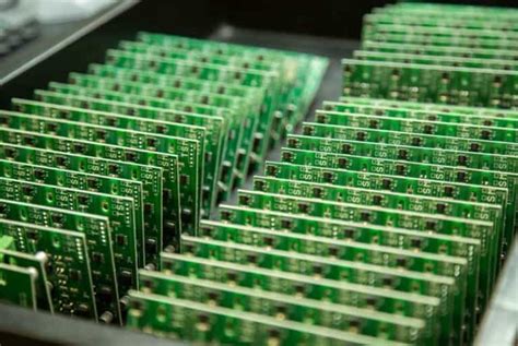
China heavy copper pcb 4 layer
Advantages Of Using China Heavy Copper PCB 4-Layer In High-Power Applications
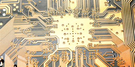
In the realm of high-power applications, the choice of printed circuit boards (PCBs) plays a pivotal role in determining the efficiency and reliability of electronic devices. Among the various options available, China heavy copper PCB 4-layer boards have emerged as a preferred choice for many engineers and manufacturers. These boards are distinguished by their enhanced current-carrying capacity, superior thermal management, and robust mechanical strength, making them particularly advantageous in demanding environments.
One of the primary advantages of using China heavy copper PCB 4-layer boards in high-power applications is their ability to handle higher currents.
Traditional PCBs often struggle with current limitations, which can lead to overheating and potential failure. However, heavy copper PCBs are designed with thicker copper layers, typically ranging from 105 to 400 micrometers, allowing them to conduct higher currents without compromising performance. This increased current-carrying capacity is crucial in applications such as power converters, automotive electronics, and industrial controls, where reliable power distribution is essential.
In addition to their current-handling capabilities, China heavy copper PCB 4-layer boards excel in thermal management.
Effective heat dissipation is a critical factor in high-power applications, as excessive heat can degrade components and reduce the overall lifespan of the device. The thick copper layers in these PCBs facilitate efficient heat transfer, minimizing the risk of hotspots and ensuring stable operation even under high thermal loads. This thermal efficiency is further enhanced by the multi-layer design, which allows for the integration of thermal vias and heat sinks, optimizing the board’s ability to manage heat.
Moreover, the mechanical strength of China heavy copper PCB 4-layer boards is another significant advantage.
The robust construction of these boards makes them highly resistant to mechanical stresses, such as bending and vibration, which are common in high-power environments. This durability ensures that the boards maintain their structural integrity over time, reducing the likelihood of mechanical failure and enhancing the reliability of the electronic device. Consequently, these boards are well-suited for applications in harsh conditions, such as aerospace and military electronics, where durability is paramount.
Furthermore, the multi-layer design of these PCBs offers additional benefits in terms of design flexibility and space optimization.
The 4-layer configuration allows for more complex circuit designs, enabling engineers to incorporate additional components and functionalities without increasing the board’s size. This compactness is particularly advantageous in applications where space is limited, such as in portable devices and compact power modules. The ability to integrate multiple functions into a single board not only saves space but also reduces the overall weight of the device, contributing to improved performance and efficiency.
In conclusion, the use of China heavy copper PCB 4-layer boards in high-power applications offers numerous advantages that enhance the performance, reliability, and efficiency of electronic devices.
Their superior current-carrying capacity, excellent thermal management, robust mechanical strength, and design flexibility make them an ideal choice for demanding environments. As technology continues to advance and the demand for high-power applications grows, the importance of selecting the right PCB cannot be overstated. By opting for China heavy copper PCB 4-layer boards, manufacturers can ensure that their devices meet the rigorous demands of modern high-power applications, ultimately leading to greater success and innovation in the field.

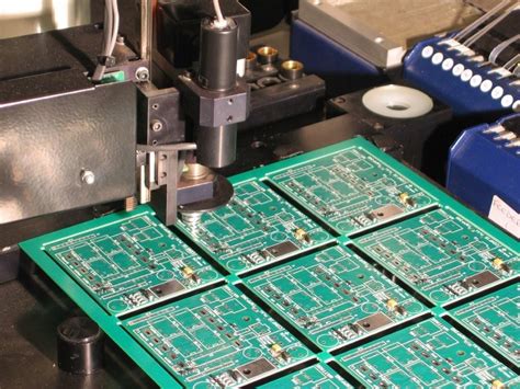
Manufacturing Process Of China Heavy Copper PCB 4-Layer: A Step-By-Step Guide
The manufacturing process of China heavy copper PCB 4-layer boards is a meticulous and intricate procedure that demands precision and expertise. This process begins with the selection of high-quality raw materials, which is crucial for ensuring the durability and performance of the final product. The base material typically consists of a fiberglass-reinforced epoxy laminate, which provides the necessary structural integrity. The copper foil, which is significantly thicker in heavy copper PCBs compared to standard ones, is then laminated onto this base material. This initial step sets the foundation for the subsequent processes.
Following the preparation of the base material, the next step involves the design and transfer of the circuit pattern onto the board.
This is achieved through a process known as photolithography. A photosensitive film is applied to the copper-clad laminate, and the desired circuit pattern is then projected onto this film using ultraviolet light. The exposed areas of the film harden, while the unexposed areas remain soft and are subsequently washed away, revealing the copper beneath. This step is critical as it defines the electrical pathways that will be etched into the copper layer.
Once the circuit pattern is established, the etching process begins.
This involves the removal of excess copper from the board, leaving only the desired circuit traces. A chemical solution, typically ferric chloride or ammonium persulfate, is used to dissolve the unwanted copper. The precision of this step is paramount, as any errors can lead to short circuits or open circuits in the final product. After etching, the board undergoes a thorough cleaning to remove any residual chemicals and debris.
The next phase in the manufacturing process is the drilling of holes for vias and mounting points.
These holes are essential for establishing electrical connections between the different layers of the PCB and for attaching components. Advanced CNC drilling machines are employed to ensure accuracy and consistency in hole placement and size. Following drilling, the holes are plated with copper to create conductive pathways between the layers, a process known as through-hole plating.
Subsequently, the board undergoes a process called layer alignment and lamination.
The individual layers of the PCB are carefully aligned and bonded together under heat and pressure. This step is crucial for ensuring that the layers are perfectly aligned, as any misalignment can lead to functional issues in the final product. The laminated board is then subjected to a series of inspections to verify its structural integrity and alignment.
The final stages of the manufacturing process involve solder mask application, surface finish, and silkscreen printing.
The solder mask, a protective layer, is applied to prevent oxidation and to insulate the copper traces. Various surface finishes, such as HASL, ENIG, or OSP, are then applied to enhance solderability and protect the copper pads. Silkscreen printing is used to apply labels and markings that aid in component placement and identification.
In conclusion, the manufacturing process of China heavy copper PCB 4-layer boards is a complex and precise operation that requires careful attention to detail at every stage. From material selection to final inspection, each step is critical in ensuring the production of high-quality PCBs that meet the rigorous demands of modern electronic applications. Through this meticulous process, manufacturers are able to deliver reliable and durable PCBs that are essential for a wide range of industries.
Comparing China Heavy Copper PCB 4-Layer With Standard PCBs: Key Differences
In the realm of printed circuit boards (PCBs), the choice of materials and design intricacies can significantly impact the performance and durability of electronic devices. Among the various types of PCBs, the heavy copper PCB, particularly the 4-layer variant, has garnered attention for its robust capabilities. When comparing China heavy copper PCB 4-layer boards with standard PCBs, several key differences emerge, each contributing to their distinct applications and advantages.
To begin with, the most notable distinction lies in the thickness of the copper used.
Standard PCBs typically feature copper thickness ranging from 1 to 3 ounces per square foot. In contrast, heavy copper PCBs, as the name suggests, utilize copper layers that can exceed 3 ounces, often reaching up to 20 ounces or more. This increased copper thickness allows heavy copper PCBs to handle higher current loads, making them ideal for applications requiring enhanced power distribution and thermal management. Consequently, industries such as automotive, aerospace, and power electronics frequently opt for heavy copper PCBs to ensure reliability and efficiency in demanding environments.
Moreover, the structural integrity of heavy copper PCBs is superior to that of standard PCBs.
The additional copper layers provide enhanced mechanical strength, which is crucial for applications subjected to mechanical stress or thermal cycling. This robustness reduces the risk of failure due to thermal expansion or contraction, thereby extending the lifespan of the device. Furthermore, the increased copper content facilitates better heat dissipation, a critical factor in preventing overheating and ensuring stable operation of high-power components.
In addition to their mechanical and thermal advantages, heavy copper PCBs offer greater design flexibility.
The ability to incorporate multiple copper layers allows for more complex circuit designs, accommodating a higher density of components and interconnections. This is particularly beneficial in compact devices where space is at a premium, yet performance cannot be compromised. The multi-layer design also enables the integration of additional features such as embedded components and blind or buried vias, further enhancing the functionality of the PCB.
Transitioning to the manufacturing process, it is important to note that producing heavy copper PCBs is more complex and requires specialized techniques compared to standard PCBs.
The increased copper thickness necessitates advanced etching and plating processes to ensure precision and quality. As a result, the production of heavy copper PCBs can be more time-consuming and costly. However, the investment is often justified by the superior performance and reliability they offer in critical applications.
Despite the higher production costs, the demand for heavy copper PCBs continues to grow, particularly in China, where advancements in manufacturing technology have made it possible to produce these boards more efficiently.
Chinese manufacturers have become leaders in the global PCB market, offering competitive pricing and high-quality products that meet international standards. This has made China a preferred destination for sourcing heavy copper PCBs, especially for companies seeking to balance cost with performance.
In conclusion, while standard PCBs suffice for many applications, the unique attributes of China heavy copper PCB 4-layer boards make them indispensable for high-performance and high-reliability applications. Their ability to handle greater current loads, withstand mechanical stress, and offer design flexibility sets them apart from their standard counterparts. As technology continues to evolve, the role of heavy copper PCBs in powering the next generation of electronic devices is poised to expand, underscoring their significance in the ever-growing electronics industry.

Design Considerations For China Heavy Copper PCB 4-Layer In Complex Circuits
When designing complex circuits, the use of China heavy copper PCB 4-layer boards presents a unique set of considerations that can significantly impact the performance and reliability of the final product. These printed circuit boards, characterized by their thick copper layers, are particularly advantageous in applications requiring high current carrying capacity and enhanced thermal management. As such, understanding the design intricacies associated with these boards is crucial for engineers aiming to optimize their circuit designs.
To begin with, the primary advantage of heavy copper PCBs lies in their ability to handle higher currents without overheating.
This is achieved through the increased thickness of the copper layers, which can range from 3 oz/ft² to over 10 oz/ft². This feature is particularly beneficial in power electronics, where efficient heat dissipation is critical. However, the increased copper thickness also necessitates careful consideration of the board’s thermal management strategies. Designers must ensure that the heat generated by the components is effectively dissipated to prevent thermal stress, which could lead to circuit failure.
Moreover, the mechanical strength of heavy copper PCBs is another factor that must be taken into account.
The robust nature of these boards makes them suitable for applications subjected to mechanical stress or harsh environmental conditions. However, this robustness also means that the boards are less flexible, which can pose challenges in certain design scenarios. Engineers must carefully plan the layout to accommodate the board’s rigidity, ensuring that the design does not compromise the board’s structural integrity.
In addition to thermal and mechanical considerations, the electrical performance of a heavy copper PCB is a critical aspect of the design process.
The increased copper thickness can lead to lower impedance and improved signal integrity, which are essential for high-frequency applications. However, this also requires precise control over the trace width and spacing to prevent issues such as crosstalk and signal loss. Designers must employ advanced simulation tools to model the electrical behavior of the circuit accurately, ensuring that the board meets the desired performance specifications.
Furthermore, the manufacturing process of heavy copper PCBs is more complex than that of standard PCBs.
The additional copper thickness requires specialized etching and plating techniques, which can increase production time and cost. Therefore, it is essential for designers to collaborate closely with manufacturers to ensure that the design is feasible and cost-effective. This collaboration can also help in identifying potential manufacturing challenges early in the design process, allowing for timely adjustments.
Finally, the choice of materials used in the construction of a heavy copper PCB is another important consideration.
The substrate material must be able to withstand the high temperatures associated with heavy copper layers, while also providing the necessary electrical insulation. Selecting the appropriate materials can enhance the board’s performance and longevity, making it a critical decision in the design process.
In conclusion, designing a China heavy copper PCB 4-layer board for complex circuits involves a careful balance of thermal, mechanical, and electrical considerations. By understanding these factors and working closely with manufacturers, engineers can create robust and efficient circuit designs that meet the demanding requirements of modern electronic applications. As technology continues to advance, the role of heavy copper PCBs in enabling high-performance circuits is likely to grow, making these design considerations increasingly relevant.