Circuit Board Assembly Services: Maximizing Reliability and Precision

Key Takeaways
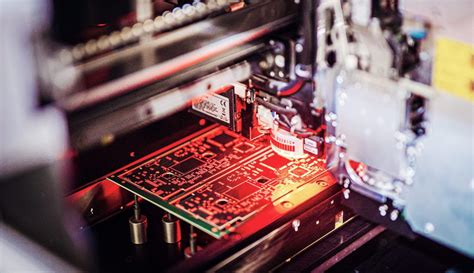
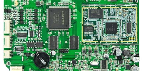
Modern PCB assembly processes rely on advanced techniques to balance speed, accuracy, and scalability. From surface-mount technology (SMT) to through-hole assembly, each PCBA method is selected based on application requirements, ensuring optimal signal integrity and thermal management. Rigorous testing protocols, such as automated optical inspection (AOI) and X-ray analysis, are embedded at every stage to minimize defects.
Tip: When evaluating PCB assembly services, prioritize providers offering end-to-end traceability and real-time quality reporting to mitigate risks in high-volume production.
Customization plays a pivotal role, with PCBA solutions tailored for industries like aerospace, medical devices, or IoT. For instance, conformal coating and hermetic sealing are critical for boards exposed to harsh environments. Meanwhile, the integration of AI-driven process optimization ensures precision in component placement, reducing human error.
Transitioning between design and manufacturing demands seamless collaboration. Advanced PCB assembly workflows now incorporate design-for-manufacturability (DFM) checks to preempt compatibility issues. This alignment between engineering and production teams not only accelerates timelines but also enhances yield rates by up to 30%.
Ultimately, the synergy of cutting-edge technology, certified standards (e.g., ISO 9001, IPC-A-610), and domain expertise defines the reliability of modern PCBA outcomes. Whether prototyping or scaling, these pillars ensure compliance with both performance benchmarks and industry regulations.
Reliable PCB Assembly Techniques
Achieving dependable PCB assembly requires a combination of advanced processes and meticulous attention to detail. Modern surface-mount technology (SMT) enables precise placement of micro-components, while automated optical inspection (AOI) systems verify solder joint integrity and component alignment in real time. For mission-critical applications, conformal coating is applied to protect assemblies from environmental stressors like moisture and dust.
A key factor in reliability lies in the use of high-temperature laminates and lead-free solder alloys, which enhance durability without compromising electrical performance. PCBA providers often employ design for manufacturability (DFM) checks to identify potential flaws early, reducing rework risks. Additionally, thermal profiling ensures even heat distribution during reflow soldering, minimizing warping or delamination.
To maintain consistency, reputable manufacturers adhere to IPC-A-610 standards for acceptability criteria, paired with rigorous in-line testing protocols. These practices not only extend product lifespans but also align with the broader emphasis on precision PCB assembly methods, forming a foundation for the next-generation technologies discussed in subsequent sections.
Precision PCB Assembly Methods
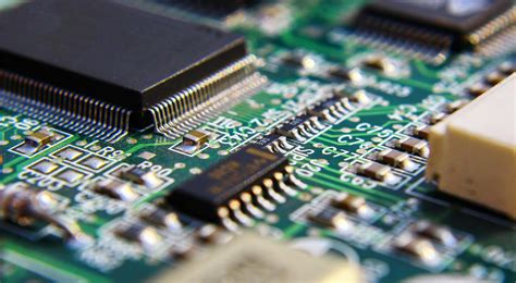
Modern PCB assembly processes demand meticulous execution to achieve the sub-millimeter tolerances required for advanced electronics. At the core of precision PCBA lies surface-mount technology (SMT), which enables the placement of miniature components—some smaller than 0.4mm—using vision-guided robotic systems. These systems achieve placement accuracies within ±25µm, critical for high-density designs in medical devices or IoT sensors.
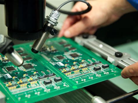
To ensure consistency, manufacturers employ automated optical inspection (AOI) systems that scan boards at 10-megapixel resolution, detecting solder defects as subtle as 15% insufficient paste volume. For complex multilayer boards, X-ray inspection verifies hidden connections in ball grid arrays (BGAs) with micron-level precision. Advanced PCB assembly workflows also integrate laser-cut stencils for solder paste application, reducing variability to under 2% across batches.
Temperature control remains paramount during reflow soldering, where thermal profiles are optimized to ±1.5°C to prevent component stress while ensuring proper intermetallic bonding. This attention to detail extends to conformal coating processes, where robotic dispensers apply protective layers with 0.1mm edge acuity. Such precision PCBA methods not only meet IPC-A-610 Class 3 standards but also support emerging applications like flexible hybrid electronics, where traditional assembly tolerances prove inadequate.
Custom PCB Assembly Solutions
Modern electronics demand tailored approaches to meet unique operational challenges, making custom PCB assembly (PCBA) indispensable for specialized applications. Unlike generic solutions, bespoke assemblies adapt to specific design requirements, whether integrating advanced sensors for medical devices or ruggedized components for aerospace systems. By leveraging pcb assembly expertise, manufacturers optimize layouts for thermal management, signal integrity, and miniaturization—critical factors in high-performance environments.
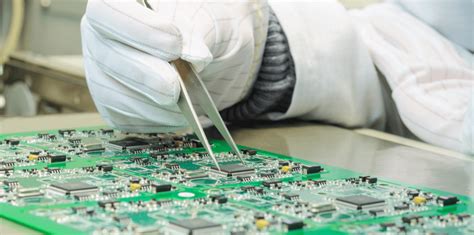
A key advantage of custom pcba lies in its flexibility. Engineers collaborate closely with clients to select materials, component placements, and soldering techniques that align with environmental conditions and end-use scenarios. For instance, automotive applications may require conformal coatings to withstand moisture, while IoT devices prioritize compact designs. Advanced pcb assembly workflows employ automated pick-and-place systems and 3D AOI (Automated Optical Inspection) to ensure micron-level precision, even for complex multi-layer boards.
Scalability further distinguishes these solutions. Providers often support low-to-mid volume production alongside rapid prototyping, enabling iterative testing without compromising timelines. This adaptability is vital for startups refining prototypes or enterprises transitioning to mass production. Additionally, custom pcba integrates seamlessly with existing quality frameworks, such as IPC-A-610 standards, to guarantee reliability across every batch. By balancing technical rigor with client-specific needs, tailored assemblies empower industries—from renewable energy to industrial automation—to innovate with confidence.
Quality Control in PCB Assembly
Effective PCB assembly relies on a multilayered quality assurance framework to ensure every PCBA meets exacting performance standards. Automated optical inspection (AOI) systems scan solder joints and component placements at micron-level accuracy, flagging deviations such as misalignments or insufficient solder paste. Complementing this, X-ray inspection verifies hidden connections in ball grid arrays (BGAs) and multilayer boards, addressing defects invisible to conventional methods.
Statistical process control (SPC) tools monitor production trends, enabling real-time adjustments to PCB assembly parameters like reflow oven temperatures or pick-and-place machine calibration. Post-assembly, functional testing simulates operational conditions—from thermal cycling to electrical load tests—to validate reliability under stress. Manufacturers adhering to IPC-A-610 and ISO 9001 standards further institutionalize consistency, documenting traceability for every batch.
For PCBA destined for aerospace or medical devices, additional protocols like contamination testing and cross-sectional analysis ensure compliance with industry-specific regulations. By integrating these strategies, suppliers minimize failure rates while aligning with the precision demands outlined in earlier sections on advanced assembly techniques.
Cutting-Edge PCB Assembly Technology
Modern PCB assembly processes leverage advancements in automation and material science to achieve unprecedented levels of precision. Automated optical inspection (AOI) systems, combined with high-resolution imaging, ensure microscopic defects are detected early, minimizing rework. Innovations like 3D solder paste inspection (SPI) further enhance accuracy by analyzing solder volume and placement before component mounting. For PCBA projects requiring ultra-fine pitch components, robotic pick-and-place machines now operate with sub-micron precision, enabling flawless integration of complex ICs and micro-BGA packages.
The adoption of laser-direct imaging (LDI) in prototyping accelerates turnaround times while maintaining tight tolerances, critical for industries like aerospace and medical devices. Additionally, advancements in surface-mount technology (SMT) allow for mixed-technology boards, seamlessly combining through-hole and surface-mounted components. To address thermal management challenges in high-density designs, manufacturers employ advanced thermal profiling during reflow soldering, ensuring optimal joint integrity.
Emerging trends such as AI-driven process optimization are reshaping PCB assembly workflows, predicting potential failures by analyzing historical production data. This synergy of cutting-edge tools and methodologies not only elevates reliability but also future-proofs PCBA solutions for evolving technological demands, aligning with Industry 4.0 standards and IoT-enabled smart manufacturing ecosystems.
Expert PCB Assembly Services
Modern PCB assembly demands specialized expertise to balance speed, accuracy, and scalability. Expert PCB assembly services combine advanced manufacturing technologies with seasoned engineering oversight to deliver mission-critical solutions for industries ranging from aerospace to medical devices. Unlike generic providers, these services prioritize PCBA (printed circuit board assembly) workflows that integrate automated pick-and-place systems, precision soldering techniques, and real-time defect detection.
A hallmark of expert providers is their ability to tailor processes to unique project requirements. For example:
| Service Feature | Standard Assembly | Expert-Level Assembly |
|---|---|---|
| Soldering Precision | ±0.1mm | ±0.02mm |
| Component Sourcing | Off-the-shelf | Customized AVL Management |
| Testing Protocols | Basic AOI | Multi-stage ICT + X-ray |
By leveraging PCBA best practices, such as thermal profiling and cross-functional DFM reviews, these services mitigate risks like solder joint fatigue or component misalignment. Moreover, certified technicians ensure compliance with IPC-A-610 and ISO 9001 standards, aligning with rigorous quality benchmarks outlined in earlier sections. This systematic approach not only enhances product longevity but also streamlines scalability for high-mix, low-volume production runs—a critical advantage in fast-evolving sectors like IoT and automotive electronics.
Industry-Specific PCB Assembly
Modern manufacturing demands PCB assembly solutions tailored to the unique requirements of different sectors. Industries such as medical devices, aerospace, automotive, and telecommunications rely on PCBA processes that align with their operational standards and regulatory frameworks. For instance, medical equipment manufacturers prioritize ultra-high precision and biocompatible materials to ensure patient safety, while automotive applications demand PCB assemblies capable of withstanding extreme temperatures and vibrations.
Specialized PCBA providers address these needs by combining adaptable manufacturing protocols with industry-specific certifications. Aerospace applications, for example, often require military-grade components and conformal coating to protect boards from harsh environmental conditions. Similarly, IoT devices in consumer electronics demand miniaturized designs with high-density interconnects. By leveraging PCB assembly expertise tailored to vertical markets, manufacturers can achieve optimal performance while complying with stringent quality benchmarks like ISO 13485 (medical) or IATF 16949 (automotive).
Transitioning between industries requires not only technical flexibility but also a deep understanding of end-use environments. This alignment ensures that PCBA outcomes meet both functional specifications and long-term reliability expectations, bridging the gap between generic production and mission-critical applications.
Rigorous PCB Testing Procedures
Modern PCB assembly processes incorporate multilayered testing protocols to ensure end-product integrity. At the core of these procedures lies automated optical inspection (AOI), which scans solder joints and component placements at micron-level accuracy. For high-density PCBA units, in-circuit testing (ICT) validates electrical performance by simulating real-world operating conditions, identifying shorts, opens, or resistance mismatches. Advanced providers also deploy functional testing, where assembled boards undergo stress scenarios mirroring their target applications—from thermal cycling in aerospace systems to vibration resistance in automotive electronics.
To minimize failure risks, PCB assembly specialists integrate statistical process control (SPC) tools, tracking critical parameters like solder paste volume and reflow oven profiles. These metrics feed into machine learning algorithms, refining tolerances for subsequent production batches. Compliance with IPC-A-610 and ISO 9001 standards further ensures that every PCBA meets industry-specific reliability benchmarks. By combining automated diagnostics with human expertise, manufacturers eliminate latent defects while maintaining alignment with client-specific performance criteria.
Conclusion
In the realm of modern electronics manufacturing, PCB assembly and PCBA processes serve as the backbone of reliable and high-performance device production. By integrating cutting-edge automation with precision engineering, advanced assembly services ensure that components meet exacting standards for functionality and durability. The emphasis on rigorous testing protocols and adaptive manufacturing workflows guarantees that each circuit board aligns with industry-specific demands, from aerospace to medical devices.
As industries evolve, the ability to deliver customized solutions while maintaining quality control remains critical. Trusted providers leverage PCB assembly expertise to address complex challenges, such as miniaturization and thermal management, ensuring seamless integration into end-use applications. Ultimately, the convergence of technological innovation and meticulous craftsmanship in PCBA not only enhances product reliability but also accelerates time-to-market for next-generation electronics. By prioritizing collaboration and continuous improvement, manufacturers can uphold the precision required to meet the dynamic needs of global markets.
Frequently Asked Questions
What distinguishes high-quality PCB assembly from standard services?
High-quality PCBA prioritizes automated optical inspection (AOI), X-ray testing, and adherence to IPC-A-610 standards to ensure component alignment, solder integrity, and long-term reliability. Standard services may lack these rigorous validation steps.
How do PCB assembly providers ensure precision for complex designs?
Advanced PCBA workflows integrate surface-mount technology (SMT), laser-cut stencils, and 3D solder paste inspection to achieve micron-level accuracy, even for high-density interconnect (HDI) boards.
Can PCB assembly services accommodate low-volume prototyping?
Yes, leading providers offer flexible production scales, combining rapid turnaround times with the same quality control protocols used for bulk orders, ensuring consistency across prototypes and mass production.
What industries benefit most from specialized PCBA solutions?
Medical devices, aerospace systems, and automotive electronics rely on industry-specific certifications (e.g., ISO 13485, IATF 16949) and environmental stress testing to meet strict performance and safety requirements.
Ready to Optimize Your Project?
For tailored PCB assembly solutions that align with your technical specifications, please click here to explore advanced PCBA capabilities and request a detailed consultation.


