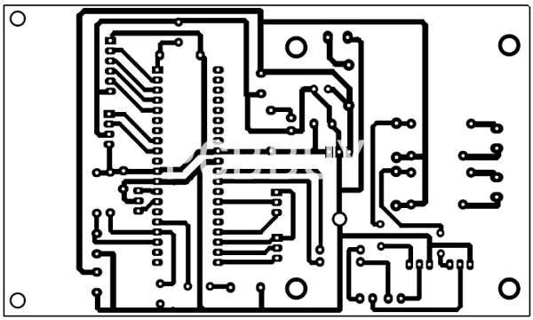
circuit board lines
PCB design wiring
Wiring, also known as Layout, is one of the most basic and important work skills for PCB design engineers. The quality of routing will directly affect the performance of the entire system. Most high-speed design theories must ultimately be implemented and verified through Layout.
It can be seen that routing is crucial in high-speed PCB design. The following will analyze the rationality of some situations that may be encountered in actual routing, and give some relatively optimized routing strategies.

Mainly from three aspects: right-angle routing, differential routing, and serpentine routing.
1. Right-angle routing
Right-angle routing is generally a situation that is required to be avoided as much as possible in PCB routing, and it has almost become one of the standards for measuring the quality of routing. So how much impact will right-angle routing have on signal transmission? In principle, right-angle routing will change the line width of the transmission line, causing impedance discontinuity. In fact, not only right-angle routing, but also angle and sharp-angle routing may cause impedance changes.
The influence of right-angle routing on signals is mainly reflected in three aspects:
First, the corner can be equivalent to the capacitive load on the transmission line, slowing down the rise time;
Second, impedance discontinuity will cause signal reflection;
Third, EMI generated by the right-angle tip Other aspects.
Of course, although the impact of right-angle routing is not very serious, it does not mean that we can all use right-angle lines in the future. Paying attention to details is the basic quality that every excellent engineer must have. Moreover, with the rapid development of digital circuits, the signal frequency processed by circuit board engineers will continue to increase. In the RF design field above 10GHz, these small right angles may become the focus of high-speed problems.
2. Differential routing
Differential signals are increasingly widely used in high-speed circuit design. The most critical signals in the circuit often adopt differential structure design. What makes it so popular? How can its good performance be guaranteed in circuit board design? With these two questions, we will discuss the next part.
What is a differential signal? In layman’s terms, the driver sends two equal and opposite signals, and the receiver determines the logic state “0” or “1” by comparing the difference between the two voltages. The pair of traces that carry differential signals is called differential traces. Compared with ordinary single-ended signal traces, the most obvious advantages of differential signals are reflected in the following three aspects:
a. Strong anti-interference ability, because the coupling between the two differential traces is very good, when there is noise interference from the outside, it is almost coupled to the two lines at the same time, and the receiver only cares about the difference between the two signals, so the common mode noise from the outside can be completely offset.
b. Can effectively suppress EMI. For the same reason, because the polarities of the two signals are opposite, the electromagnetic fields they radiate to the outside can offset each other. The tighter the coupling, the less electromagnetic energy is released to the outside.
c. Accurate timing positioning. Because the switching change of the differential signal is located at the intersection of the two signals, unlike the ordinary single-ended signal that relies on the high and low threshold voltages for judgment, it is less affected by the process and temperature, which can reduce the timing error, and is also more suitable for circuits with low amplitude signals. The currently popular LVDS (low voltage differential signaling) refers to this small amplitude differential signal technology. More related knowledge: www.jiepei.com/G588
For circuit board engineers, the most important concern is how to ensure that these advantages of differential routing can be fully utilized in actual routing. Perhaps anyone who has been exposed to Layout will understand the general requirements of differential routing, that is, “equal length and equal distance”.
Equal length is to ensure that the two differential signals always maintain opposite polarity and reduce common mode components; equal distance is mainly to ensure that the differential impedance of the two is consistent and reduce reflection.
“The principle of keeping as close as possible” is sometimes also one of the requirements for differential routing. But all these rules are not used to apply mechanically, and many engineers do not seem to understand the essence of high-speed differential signal transmission.
GET PCB MANUFACTURING AND ASSEMBLY QUOTE NOW!
The following focuses on several common misunderstandings in circuit board differential signal design.
Misunderstanding 1: It is believed that differential signals do not need a ground plane as a return path, or that differential routing provides a return path for each other.
The reason for this misunderstanding is that they are confused by surface phenomena or that the mechanism of high-speed signal transmission is not deeply understood.
The partial return cancellation of the ground plane does not mean that the differential circuit does not use the reference plane as the signal return path. In fact, in the signal return analysis, the mechanism of differential routing and ordinary single-ended routing is the same, that is, high-frequency signals always return along the loop with the smallest inductance.
The biggest difference is that in addition to the coupling to the ground, the differential lines also have mutual coupling. The one with the stronger coupling becomes the main return path. In the circuit design of the circuit board, the coupling between the differential routing is generally small, often accounting for only 10~20% of the coupling degree, and more is the coupling to the ground, so the main return path of the differential routing still exists in the ground plane.
When the ground plane is discontinuous, in the area without the reference plane, the coupling between the differential routing will provide the main return path. Although the discontinuity of the reference plane does not have as serious an impact on differential routing as it does on ordinary single-ended routing, it will still reduce the quality of differential signals and increase EMI, so it should be avoided as much as possible.
Some designers also believe that the reference plane under the differential routing can be removed to suppress some common-mode signals in differential transmission, but theoretically this approach is not advisable. How to control impedance? Not providing a ground impedance loop for common-mode signals will inevitably cause EMI radiation, which is more harmful than beneficial.
Misunderstanding 2: It is believed that maintaining equal spacing is more important than matching line length. In actual circuit board wiring, the requirements of differential design cannot often be met at the same time.
Due to factors such as pin distribution, vias, and routing space, appropriate winding must be used to achieve the purpose of line length matching, but the result is that some areas of the differential pair cannot be parallel. How should we choose at this time?
The impact caused by unequal spacing is minimal. In comparison, the impact of mismatched line length on timing is much greater.
From a theoretical analysis, although inconsistent spacing will cause changes in differential impedance, the impedance change range is also very small because the coupling between differential pairs is not significant, usually within 10%, which is equivalent to the reflection caused by a via, which will not have a significant impact on signal transmission.
Once the line length is mismatched, in addition to the timing offset, common mode components are introduced into the differential signal, reducing the signal quality and increasing EMI.
It can be said that the most important rule in the design of differential traces on circuit boards is to match the line length, and other rules can be flexibly handled according to design requirements and practical applications.
misunderstanding 3: It is believed that differential traces must be very close. Bringing differential traces close is nothing more than enhancing their coupling, which can not only improve immunity to noise, but also make full use of the opposite polarity of the magnetic field to offset the electromagnetic interference to the outside world.
Although this approach is very beneficial in most cases, it is not absolute. If we can ensure that they are fully shielded and not interfered by the outside world, then we don’t need to achieve the purpose of anti-interference and EMI suppression through strong coupling with each other.
How can we ensure that differential traces have good isolation and shielding? Increasing the spacing between other signal traces is one of the most basic ways. The energy of the electromagnetic field decreases in a square relationship with the distance.
Generally, when the line spacing exceeds 4 times the line width, the interference between them is extremely weak and can be basically ignored. In addition, the isolation through the ground plane can also play a good shielding role.
This structure is often used in the design of high-frequency (above 10G) IC packaging circuit boards. It is called the CPW structure, which can ensure strict differential impedance control (2Z0). Differential traces can also be run in different signal layers, but this method is generally not recommended because the differences in impedance and vias generated by different layers will destroy the effect of differential mode transmission and introduce common mode noise.
In addition, if the coupling between two adjacent layers is not tight enough, the ability of the differential trace to resist noise will be reduced, but if the appropriate spacing from the surrounding traces can be maintained, crosstalk will not be a problem. At normal frequencies (below GHz), EMI will not be a serious problem.
Experiments show that the radiation energy attenuation of differential traces 500 Mils apart at 3 meters has reached 60 dB, which is enough to meet the FCC’s electromagnetic radiation standards. Therefore, designers do not need to worry too much about electromagnetic incompatibility caused by insufficient differential line coupling.
3. Serpentine line
Serpentine line is a type of routing method often used in Layout. Its main purpose is to adjust the delay and meet the system timing design requirements.
Designers must first have such an understanding: Serpentine line will damage the signal quality and change the transmission delay, and should be avoided as much as possible during wiring.
However, in actual design, in order to ensure that the signal has enough hold time or reduce the time offset between the same group of signals, it is often necessary to deliberately wind the line. So, what effect does the serpentine line have on signal transmission?
What should be paid attention to when routing?
The two most critical parameters are the parallel coupling length (Lp) and the coupling distance (S). Obviously, when the signal is transmitted on the serpentine line, coupling will occur between the parallel line segments in the form of differential mode.
The smaller the S and the larger the Lp, the greater the degree of coupling. It may lead to a reduction in transmission delay and greatly reduce the quality of the signal due to crosstalk.
Here are some suggestions for layout engineers when dealing with serpentine lines:
1. Try to increase the distance (S) of parallel line segments to at least 3H, where H refers to the distance from the signal line to the reference plane. In layman’s terms, it means routing around a large bend. As long as S is large enough, the mutual coupling effect can be almost completely avoided.
2. Reduce the coupling length Lp. When the delay of twice the Lp approaches or exceeds the signal rise time, the crosstalk generated will reach saturation.
3. The signal transmission delay caused by the serpentine line of strip-line or embedded micro-strip is smaller than that of micro-strip. In theory, the transmission rate of strip-line will not be affected by differential-mode crosstalk.
4. For high-speed signal lines and signal lines with strict timing requirements, try not to use serpentine lines, especially not to meander in a small range.
5. Serpentine routing at any angle can be often used to effectively reduce mutual coupling.
6. In high-speed circuit board design, serpentine routing has no so-called filtering or anti-interference ability, and can only reduce signal quality, so it is only used for timing matching and has no other purpose.
7. Sometimes you can consider winding in the form of spiral routing. Simulation shows that its effect is better than normal serpentine routing.
GET PCB AND ASSEMBLY SERVICE QUOTE NOW!
How to reasonably layout analog circuit printed circuit board signal lines
There is a recognized rule that in all analog circuit printed circuit boards, signal lines should be as short as possible. This is because the longer the signal line, the more inductive and capacitive donations in the circuit, which is not desirable.
The reality is that it is impossible to make all signal lines as short as possible. Therefore, the first thing to consider when wiring is the signal line that is most likely to cause interference.
In analog circuit printed circuit boards, signal lines can perform various functions, such as signal input, feedback, output, and providing reference signals.
Therefore, for different applications, signal lines must be optimized in various ways. However, there is a generally accepted rule that in all analog circuit printed circuit boards, signal lines should be as short as possible, because the longer the signal line, the more inductive and capacitive contributions there are in the circuit, which is undesirable.
The reality is that it is impossible to make all signal lines as short as possible, so the first thing to consider when wiring is the signal line that is most likely to cause interference.
In particular, the wiring of signal lines in the following circuits requires special attention:
1) High-frequency amplifier/oscillator;
2) Multi-stage amplifier, especially amplifier with higher output power;
3) High-gain DC amplifier;
4) Small signal amplifier;
5) Differential amplifier.
1. High-frequency amplifier/oscillator
If the wiring of the high-frequency amplifier printed circuit board is unreasonable, the bandwidth of the amplifier will be reduced. This is because a large capacitor will be formed between two close ground lines and signal lines, and this capacitor together with the output resistor will form a low-pass filter.
This low-pass filter reduces the bandwidth of the amplifier. At the same time, if the input signal line and the output signal line are close to each other, the feedback signal will cause oscillation. In order to avoid these problems, there should be enough space between the above wires.
Electronic circuit designers usually have a common experience that if they design a high-frequency amplifier, it will actually oscillate. Similar problems will also be encountered in the layout of the oscillator, which does not oscillate at the designed frequency.
This problem is caused by the capacitive coupling between the signal lines. Therefore, it is very important to reduce the coupling capacitance between the signal lines when laying out the printed circuit board.
2. Multi-stage amplifier with high power output
If the power line and ground line are too long, the multi-stage amplifier is prone to low-frequency oscillation. Because the wires themselves have resistivity, the large current caused by the high power output will flow through these wires.
Adding a large enough capacitor between the power supply and the ground to form a power decoupling circuit can solve this problem. Alternatively, provide independent power and ground lines for different amplifier stages, so that there will be no common power and ground line paths.
3. High-gain DC amplifier
High-gain DC amplifiers are usually used for small signal amplification. When devices such as transistors or DC amplifiers are soldered on a printed circuit board, thermocouples are formed at the connection between the copper tube and the device pins, thereby generating different alternating voltages, forming an interference signal for the amplifier.
In order to minimize the temperature change rate around the input stage of the DC amplifier and keep it constant, it is recommended to surround the input stage with an isolation device to avoid the influence of air flow around it.
4. Small signal amplifier
This signal amplifier processes small signals and includes the following two types.
(1) High impedance (low current) amplifier
In this amplifier, there is capacitive coupling between two adjacent signal lines, which will seriously affect the performance of the circuit and even cause low-level signals to be covered. In a high-impedance circuit, there is capacitive coupling between two wires. In order to reduce coupling, it is recommended to keep a sufficient distance between high-impedance signal lines and other interfering signals. Generally, this distance
At least 40 times the signal line width.
In any case, the capacitance of low-level signal lines to ground should be high to reduce coupling voltage. That is, the low-level signal conductors should be close to the ground line. If sufficient width between low-level signal lines cannot be guaranteed, a ground line can be laid between them to reduce coupling.
When the amplifier uses a photocell or chemical battery as a power source, the power supply impedance can reach millions or even hundreds of millions of ohms. If the printed circuit board is not fully cleaned after etching, the electrolyte remaining on the surface of the circuit board will produce a large resistance between adjacent conductors.
Even if the circuit board is completely cleaned, there is still a leakage resistance of no more than 10 12 0. Moreover, these resistances cannot be distributed isotropically, so that the resistance between two adjacent conductors may be higher than the resistance between two conductors farther apart.
Therefore, the input of the low-level I1 V (current/voltage) converter should be protected by a guard loop on both sides of the printed circuit board, and the guard loop should be connected to a point with the same potential as the main connection point. If this is done, the exact value of the leakage resistance is not so important because the differential voltage applied to it is already very small.
High impedance amplifier printed circuit boards cannot use plated through holes. The volume resistivity of printed circuit board materials is lower than the surface resistivity, and it is difficult to install guard rings on the substrate.
The best method is to connect the terminals of the high impedance amplifier to the Teflon insulator rather than the printed circuit board wires.
(2) Low impedance (low voltage) amplifier
In low impedance circuits, induced voltage may be generated because of the presence of inductive coupling or magnetic fields in the circuit. This interference can be reduced to a certain extent by the following methods:
1) Keep the high-level AC signal line and the low-level signal line at a sufficient distance;
2) Lay the ground wire near the signal line;
3) Avoid forming a ground loop to prevent external magnetic fields from interfering with the low-level signal.
5. Differential amplifier
The differential amplifier only amplifies the difference between two signals, and will not amplify their common voltage signal. If the differential amplifier and printed circuit board are not designed properly, when the signal level is low, the common voltage will generate a small differential interference signal.
The input impedance of the differential amplifier is high, and any imbalance in the input parameters will cause great interference to the circuit. Therefore, when designing the printed circuit board, it is necessary to ensure that the amplifier is completely symmetrical in physical structure.
There is a certain leakage resistance at the input of the differential amplifier, which can cause unbalanced voltage offset. This problem can be solved by adding a guard to the input circuit. The guard surrounds the signal line, and if it can maintain the same voltage as the low-level end of the two input signal lines, it will cause an increase in effective resistance.
This device can ensure that the signal source terminal and the guard are at the same level as the low-level end of the signal source.
The guard line should form a loop, surround the signal line from the input end to the input connection point of the amplifier, and be connected to the guard of the equipment, which is an effective method for processing low-level differential signals. In addition, the printed circuit board substrate of the small signal differential amplifier is more suitable for epoxy glass material, which helps to reduce leakage current.