Circuit board testing, inspection and specifications
1.Acceptability, acceptance
The former refers to the various operating conditions and written criteria that should be followed when inspecting semi-finished or finished products. The latter refers to the process of performing acceptance inspection, such as Acceptance Test.
2.Acceptable Quality Level (AQL)
Acceptable Quality Level
It refers to the “upper limit of defective rate” that the inspected batch is considered to meet the engineering requirements during random inspection, or the upper limit of the percentage of defects. AQL is not set to protect a particular batch, but a guarantee for the quality of continuous batches.
3.Air Inclusion
When the board is coated with liquid materials, there are often bubbles remaining in the coating, such as bubbles in film resin, or bubbles in green paint printing film, etc. Such mixed bubbles are very bad for the electrical or physical properties of the board.
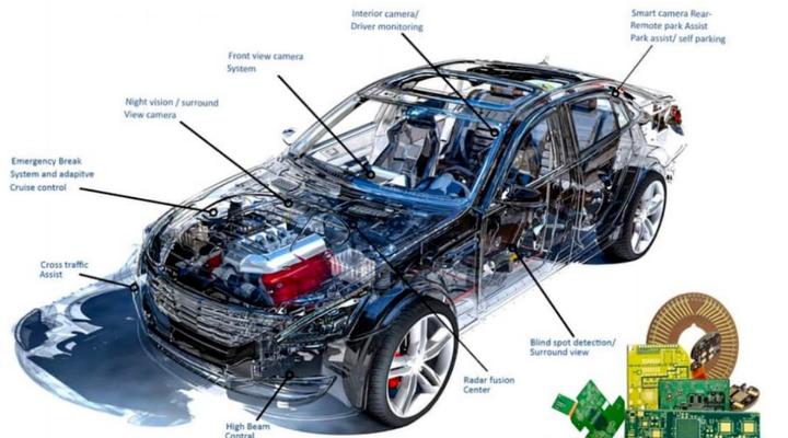
4.AOI Automatic Optical Inspection
Automatic Optical Inspection is an optical device that uses ordinary light or laser light with computer programs to visually inspect the appearance of the circuit board surface to replace manual visual inspection.
5.AQL Acceptable Quality Level
Acceptable Quality Level is a quality control technology that selects a small amount of products for inspection in the quality inspection items of a large number of products, and then determines the trend of the entire batch based on it.
6.ATE Automatic Electrical Testing Equipment
In order to ensure the smoothness of the circuit system of the completed circuit board, it is necessary to use a needle disk with specific contacts on a general-purpose electrical testing mother machine with high voltage (such as 250 V) and multiple test points to conduct electrical testing on the board. This general-purpose testing machine is called Automatic Testing Equipment.
7.Blister Local delamination or blistering
In the circuit manufacturing process, delamination of local board surfaces or local board materials, or local copper foil floating, often occurs, which is called Blister. In addition, in the general electroplating process, blistering of the coating often occurs due to unclean substrate treatment, especially for silver-plated objects that are most likely to bubble during post-baking.
8.Bow, Bowing
When the board loses its flatness, it is placed on a flat table with its concave surface facing down. If the four corners of the board cannot be kept on the same plane, it is called warp or warpage. If only three points can fall on the plane, it is called twist. However, this twist is usually very mild and not very obvious, and it is commonly called warpage.
9.Break-Out
It means that the drilled hole has broken out of the pad to form a broken ring; that is, the hole position and the pad to be drilled are not aligned, so that the two centers do not fall on one point. Of course, both drilling and image transfer may be the cause of misalignment or breakout. However, it is impossible to align each of the thousands of holes on the board. As long as there is no “breakout” and the narrowest part of the hole ring is not lower than the specification (generally more than 2 mil), it can be accepted.
10.Bridging
Refers to the improper short circuit between two lines that should be isolated from each other.
11.Certificate
When a specific “personnel training” or “quality test” is completed and meets a certain professional standard, a document that is specially recorded in writing to certify it is called a Certificate.
12.Check List
In a broad sense, it refers to the items that should be checked one by one for safety considerations before various operations. In a narrow sense, it refers to the various items that are checked one by one in the PBC industry when customers come to the site to understand the quality.
13.Continuity
Refers to whether the current in the circuit (Circuits) flows smoothly. Continuity Testing refers to the test of the power supply of each circuit, that is, find two points at both ends of each circuit, make tight contact with them with elastic probes (implemented with a needle bed for the entire board), and then apply a specified voltage (usually twice the practical voltage) to perform a “connectivity test”, which is commonly known as Open/Short Testing.
14.Coupon, Test Coupon Board Edge Sample
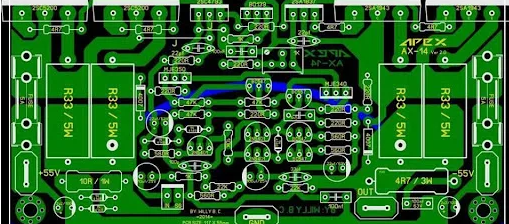
To understand the detailed quality of the circuit board, especially the through-hole structure of the multi-layer board, it is not enough to rely on appearance inspection and electrical testing, but also to conduct further micro-sectioning (Microsectioning) microscopic inspection of its structure. Therefore, it is necessary to set up additional “through-hole and circuit” patterns at one or more places on the edge of the board as anatomical sections and conformal coupons (Conformal Coupons) to monitor the structural integrity (Structure Integraty) of the board. For those with particularly strict quality, if the cutting sample fails, the board will not be shipped. Note: This board edge slicing can not only be used as a product inspection item for shipment, but also as a countermeasure research for problems and a monitoring tool for quality improvement. In addition to micro-slice samples, a special coupon for checking “characteristic impedance” is sometimes added to the board edge to check whether the “impedance value” of each multilayer board is still controlled within the specified range.
15.Crazing
It refers to the defects on the appearance of the substrate. It may be due to the split between the local glass fiber cloth and epoxy resin, or between the yarn bundles of the cloth itself. The white area visible on the surface is called Crazing. Smaller ones that only appear on the weaving points are called “white spots” (Measling). In addition, when the protective film (Conformal Coating) applied on the surface of the assembled board is cracked, it is also called Crazing. Usually, ordinary daily necessities porcelain or tiles, after long-term use and aging, also have irregular cracks on the surface due to the release of force, which is also called Crazing.
16.Crosshatch Testing
It is a destructive test of the adhesion of the board surface film. It is based on the ASTM D3359 tape tearing method and slightly modified to test the adhesion of various wet and dry films on the board surface. A multi-blade cutting knife is used to cut vertically and horizontally on the film surface, cut into many small squares, and then press with tape and tear them up. 5 points are given to those with smooth cuts and no tearing. Only 1 point is given to those with 35-65% of the cuts and the squares are torn up, and 0 points are given to those with worse. Do it several times for comparison, and the total score is the score of the film adhesion.
17.Dendritic Growth
It refers to the dendritic growth of metal ions between two conductors on the circuit board in a humid environment and under the influence of long-term voltage (bias), and finally cross the insulating board surface to form a lap, causing leakage or short circuit, which is called “dendritic growth”. When it continuously penetrates into the insulating material, it is called Dendritic Migration or Dentrices.
18.Deviation
The measured data is not good, and the gap between it and the normal acceptance specification is called Deviation.
19.Eddy Current
In the PCB industry, it is a working principle and method for measuring the thickness of various films. It can measure the thickness of non-conductive films of non-magnetic metal substrates (such as the resin layer or green paint thickness on the copper surface). When a coil is wound on a probe (Probe) with an iron core, a high-frequency oscillating alternating current (100KHz~6MHz) is applied to generate a magnetic field. When the probe contacts the surface to be measured, the bottom metal layer (such as copper) will be induced to generate “eddy current”, and the signal of this eddy current will be detected by the probe. The thicker the non-conductive film on the surface, the greater the effect of blocking eddy current, making the signal that the probe can receive weaker. On the contrary, the thinner the film is, the stronger the signal the probe can receive. Therefore, this principle can be used to measure the thickness of non-conductive films. Generally, the thickness of the anodized film on the surface of aluminum materials, the thickness of the substrate on the copper foil substrate, and any similar combination can be measured. Eddy currents are also generated in general circuit systems, but they are invalid currents that can only generate heat and are wasted.
20.Dish Down
It refers to the local area on the copper conductor line on the circuit board surface, which is improperly circularly depressed during pressing, and after etching, it is still left on the line, which is called “dish down”. In high-speed transmission lines, this local depression will cause a sudden change in impedance value, which is not good for the overall function, so it should be avoided as much as possible