Circuit Card Assembly Design: Best Practices for Efficiency and Precision

Key Takeaways
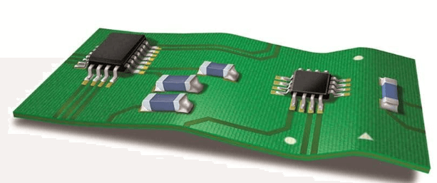
Effective PCB assembly and PCBA design hinge on balancing efficiency with precision across multiple stages of development. A well-structured component layout minimizes signal interference and reduces production bottlenecks, particularly when integrating high-density interconnects. Advanced soldering techniques, such as reflow or selective wave soldering, ensure robust electrical connections while accommodating miniaturized components.
Thermal management remains a critical focus, with thermal vias and heat sinks strategically placed to dissipate energy in high-power circuits. For precision, automated pick-and-place systems paired with laser-aligned mounting enhance alignment accuracy, reducing manual calibration errors. Compliance with IPC-A-610 standards guarantees reliability, particularly in applications demanding extended operational lifespans.
Material selection directly impacts performance—high-Tg substrates and low-loss dielectrics are increasingly prioritized for thermally demanding environments. Additionally, implementing design-for-manufacturability (DFM) principles early in the PCBA workflow prevents costly revisions. Rigorous quality control protocols, including automated optical inspection (AOI) and X-ray testing, validate consistency across production batches. By harmonizing these strategies, engineers achieve fault-tolerant designs that meet both technical specifications and cost-efficiency targets.

Optimizing Component Layout Strategies
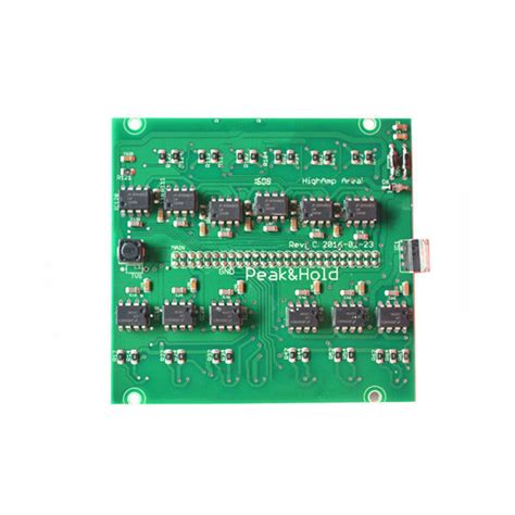
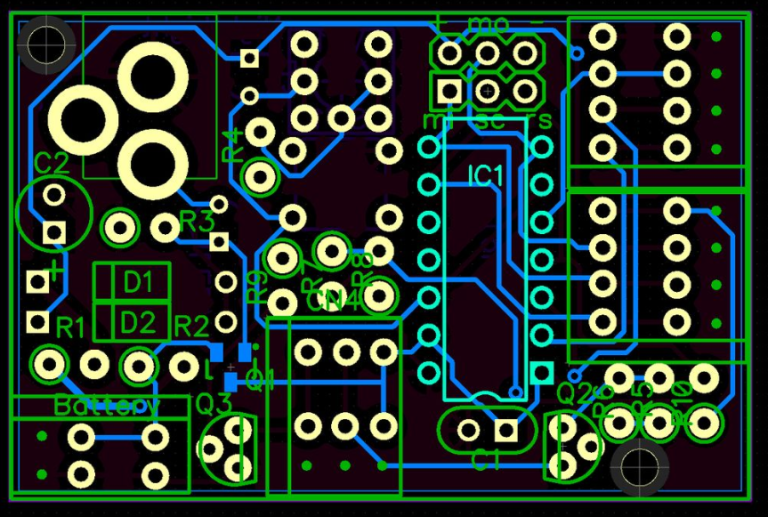
Effective PCB assembly begins with strategic component placement, a critical factor influencing both manufacturing efficiency and end-product performance. When designing a PCBA layout, engineers must balance spatial constraints with electrical requirements to minimize signal interference and thermal bottlenecks. Grouping components by functional blocks reduces trace lengths, lowering parasitic capacitance and inductance—key considerations for high-frequency applications.
A well-optimized layout prioritizes thermal management by positioning heat-generating components, such as voltage regulators or power amplifiers, away from temperature-sensitive elements like crystal oscillators. This spatial separation, combined with judicious use of thermal vias and copper pours, ensures even heat dissipation across the board. For mixed-signal designs, partitioning analog and digital sections with guard traces or isolation gaps prevents cross-talk, preserving signal integrity.
In PCB assembly workflows, design for manufacturability (DFM) principles dictate maintaining standardized component orientations to streamline pick-and-place operations. Aligning polarized parts in consistent directions reduces machine recalibration time during PCBA production. Additionally, reserving adequate clearance between surface-mount devices (SMDs) prevents solder bridging, particularly for fine-pitch ICs or micro-BGA packages.
Advanced CAD tools now incorporate automated design rule checks (DRCs) to flag potential assembly conflicts, such as insufficient pad sizes or improperly spaced vias. However, human expertise remains vital for evaluating trade-offs between automated suggestions and application-specific requirements. For instance, high-current paths may necessitate wider traces despite spatial constraints, while RF circuits demand precise impedance-controlled routing.
Implementing these strategies not only accelerates PCB assembly timelines but also enhances long-term reliability. By reducing mechanical stress through symmetrical component distribution and avoiding board-edge placements, designers mitigate risks of solder joint fatigue—a common failure mode in vibration-prone environments. As PCBA complexity grows with IoT and miniaturization trends, optimized layouts become indispensable for achieving repeatable precision in volume production.

Advanced Soldering Methods Explained
Modern PCB assembly relies heavily on advanced soldering techniques to ensure electrical connectivity and mechanical stability in PCBA (Printed Circuit Board Assembly). Among the most impactful methods are reflow soldering and wave soldering, each tailored for specific component types and production scales. Reflow soldering, ideal for surface-mount devices (SMDs), uses precisely controlled heating profiles to melt solder paste, creating reliable joints without damaging heat-sensitive components. For through-hole components, wave soldering remains a staple, where boards pass over a molten solder wave to form durable connections.
Tip: When selecting a soldering method, consider the thermal tolerance of components. For mixed-technology boards combining SMDs and through-hole parts, a hybrid approach—such as selective soldering—can optimize efficiency while minimizing thermal stress.
Emerging technologies like laser soldering are gaining traction in high-precision PCBA applications. This method employs focused laser beams to achieve micron-level accuracy, particularly useful for fine-pitch components or densely packed designs. Additionally, vapor phase soldering offers uniform heat distribution, reducing the risk of warping in complex multilayer boards.
Material selection plays a critical role here. High-quality solder alloys with low voiding rates, paired with no-clean flux formulations, enhance joint reliability and reduce post-assembly cleaning requirements. For mission-critical applications, X-ray inspection and automated optical inspection (AOI) systems are indispensable for detecting solder defects like bridging or cold joints.
To balance speed and precision, many manufacturers now integrate automated soldering robots equipped with vision systems. These systems adjust parameters in real time, compensating for component placement variances and ensuring consistent results across high-volume PCB assembly runs. By aligning method selection with design requirements, engineers can significantly improve yield rates and long-term product performance.
Thermal Management in PCB Assembly
Effective thermal management is critical in PCB assembly to ensure long-term reliability and optimal performance of electronic devices. As component densities increase and power requirements grow, managing heat dissipation becomes a central challenge in PCBA design. Without proper thermal controls, excessive temperatures can lead to component degradation, signal integrity issues, and even catastrophic failures.
A strategic approach begins with component placement optimization. High-power components like voltage regulators or processors should be positioned to minimize localized heat accumulation. For example, placing heat-generating parts near board edges or adjacent to dedicated cooling features enhances airflow. Additionally, integrating thermal vias—small plated holes that transfer heat to inner layers or heatsinks—helps distribute thermal energy efficiently.
| Thermal Management Technique | Application | Impact on Performance |
|---|---|---|
| Copper pours | Dissipate heat across ground planes | Reduces localized hotspots by 15-20% |
| Thermal interface materials | Connect components to heatsinks | Lowers thermal resistance by 30-40% |
| Active cooling systems | Integrate fans or liquid cooling | Enhances heat dissipation capacity by 50%+ |
Advanced PCBA designs also leverage materials engineered for thermal efficiency. For instance, substrates with high thermal conductivity (e.g., metal-core or ceramic-filled laminates) improve heat transfer, while solder masks with low thermal expansion coefficients reduce mechanical stress during temperature fluctuations.
In high-frequency or industrial applications, simulations using computational fluid dynamics (CFD) predict airflow patterns and thermal behavior, enabling preemptive adjustments. Post-assembly, infrared thermography validates thermal performance, ensuring compliance with industry standards like IPC-2221.
By balancing material selection, layout strategies, and validation protocols, engineers achieve thermal equilibrium in PCB assembly, directly contributing to enhanced product lifespan and operational stability. This integration of proactive design and rigorous testing aligns with broader goals of manufacturing precision and reliability in modern electronics.
Precision Assembly Process Optimization
At the core of high-performance PCB assembly lies the meticulous orchestration of precision-driven workflows. Modern PCBA manufacturing demands a harmonized approach that integrates automated placement systems with rigorous process controls. For instance, advanced pick-and-place machines equipped with vision-guided alignment achieve micron-level accuracy, reducing positional deviations to less than ±0.025mm. This is particularly critical for fine-pitch components, where even minor misalignments can compromise electrical connectivity or thermal dissipation.
A key strategy involves optimizing solder paste application through laser-etched stencils and real-time volumetric inspection. By maintaining a consistent paste deposition thickness (typically 80–120μm), manufacturers minimize defects like bridging or insufficient joints during reflow soldering. Pairing this with nitrogen-enriched reflow ovens further enhances wetting behavior, yielding smoother intermetallic layers that bolster long-term reliability.
Another critical aspect is the adoption of closed-loop feedback systems in PCB assembly lines. In-line automated optical inspection (AOI) and X-ray tomography immediately flag anomalies, enabling dynamic adjustments to placement pressure or thermal profiles. For example, thermal profiling tools track board-specific heating rates during reflow, ensuring components with varied mass—such as BGAs and MLCCs—reach optimal peak temperatures without exceeding their thermal stress thresholds.
To maintain precision at scale, lean methodologies like Six Sigma are applied to PCBA workflows. Statistical process control (SPC) charts monitor critical parameters—component coplanarity, solder ball size, and void percentages—against predefined tolerances. This data-driven approach reduces process variability by up to 40%, as evidenced in high-density interconnect (HDI) board production.
Finally, integrating design for manufacturability (DFM) principles early in the design phase prevents assembly challenges. Collaboration between design engineers and PCB assembly technicians ensures pad geometries, component spacing, and fiducial marker placements align with the capabilities of automated systems, eliminating costly rework cycles.
Ensuring Circuit Board Reliability Standards
Achieving consistent reliability in PCB assembly requires adherence to industry-proven protocols and rigorous testing methodologies. At the core of dependable PCBA performance lies the integration of design-for-reliability (DFR) principles, which prioritize fault-tolerant layouts and material compatibility. A critical first step involves selecting substrates with optimal thermal expansion coefficients to minimize stress during temperature fluctuations, a common failure point in high-density designs.
To mitigate risks, manufacturers employ automated optical inspection (AOI) systems to detect micro-cracks or misaligned components post-soldering, ensuring compliance with IPC-A-610 standards. For mission-critical applications, accelerated life testing simulates years of operational stress within controlled environments, validating PCB assembly durability under extreme humidity, vibration, or thermal cycling conditions.
Strategic PCBA reinforcement techniques, such as conformal coating and underfill encapsulation, provide additional protection against environmental contaminants and mechanical fatigue. Recent advancements in predictive analytics now enable real-time monitoring of solder joint integrity, allowing preemptive maintenance before catastrophic failures occur.
Transitioning from design to production, maintaining traceability through serialized component tracking ensures quick root-cause analysis if field issues emerge. By aligning material choices with operational requirements—such as high-Tg laminates for automotive applications or halogen-free substrates for aerospace—engineers balance reliability with regulatory compliance.
This focus on proactive quality assurance not only reduces warranty claims but also strengthens brand reputation in competitive electronics markets. As miniaturization trends push PCB assembly boundaries, integrating these reliability safeguards becomes paramount for sustaining performance in next-generation IoT and AI-driven devices.
Efficiency in Circuit Card Design
Achieving efficiency in circuit card design requires a holistic approach that balances PCB assembly timelines with performance requirements. A critical starting point is optimizing component placement to minimize trace lengths, which reduces signal interference and power loss. By strategically grouping high-frequency components and isolating noise-sensitive circuits, designers can enhance signal integrity while accelerating PCBA workflows.
The integration of automated design tools plays a pivotal role in streamlining layouts. Modern software enables rapid prototyping by simulating thermal profiles and electrical performance, allowing engineers to preemptively address bottlenecks. For instance, incorporating thermal vias near heat-generating components during the design phase ensures efficient heat dissipation, reducing the need for post-production modifications.
Material selection also impacts efficiency. Using standardized surface-mount technology (SMT) components not only simplifies PCB assembly but also improves compatibility with automated pick-and-place systems. Additionally, adopting design for manufacturability (DFM) principles—such as maintaining consistent pad sizes and avoiding acute angles in traces—reduces errors during PCBA soldering processes.
Time-to-market pressures demand agile design iterations. Implementing modular layouts, where functional blocks can be reused across projects, slashes development cycles by up to 30%. Pairing this with real-time collaboration between design and manufacturing teams ensures alignment on tolerances and material specifications, mitigating delays caused by redesigns.
Finally, leveraging data-driven analytics to monitor production yields helps refine design rules. For example, tracking failure rates of specific PCB assembly steps can reveal patterns tied to component density or soldering parameters, enabling proactive adjustments. By embedding efficiency into every design decision, engineers achieve precision without compromising scalability.
PCB Manufacturing Quality Control
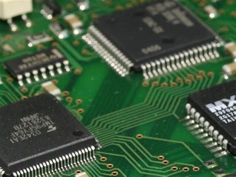
Maintaining rigorous quality control protocols is paramount in PCB assembly processes to ensure consistent performance and longevity of electronic devices. A robust quality framework begins with automated optical inspection (AOI) systems, which scan PCBA layers for soldering defects, misaligned components, or trace irregularities. These systems achieve micron-level accuracy, identifying issues like cold joints or bridging that could compromise electrical connectivity.
Statistical process control (SPC) methods further enhance reliability by analyzing production data in real time, enabling rapid adjustments to soldering temperatures or pick-and-place machine calibration. For high-density boards, X-ray inspection becomes critical to verify BGA (ball grid array) solder connections hidden beneath components—a step often mandated in aerospace or medical PCBA applications.
Material integrity is another focal point. Quality teams test substrate laminates for thermal expansion coefficients and dielectric strength, ensuring compatibility with operational environments. Solder mask adhesion tests and copper thickness measurements prevent delamination or signal loss risks.
To validate assembly consistency, manufacturers implement environmental stress testing, exposing PCB assemblies to extreme temperatures, humidity, and vibration cycles. This simulates decades of field use within hours, revealing potential failure points in thermal management systems or component mounting.
Finally, electrical testing validates functional performance. Flying probe testers and boundary-scan tools check for open circuits, short circuits, and signal integrity deviations. By integrating these strategies, PCB assembly workflows achieve defect rates below 50 ppm, aligning with ISO 9001 and IPC-A-610 standards for mission-critical electronics.
Material Selection for Optimal Performance
The foundation of reliable PCB assembly begins with strategic material selection, a process that directly impacts electrical performance, thermal stability, and long-term durability. In PCBA manufacturing, substrate materials like FR-4 epoxy laminates remain industry standards for their balanced dielectric properties and cost-effectiveness, while high-frequency applications demand specialized polyimide or PTFE-based substrates to minimize signal loss.
Copper foil thickness and surface finish choices—such as HASL (Hot Air Solder Leveling) or ENIG (Electroless Nickel Immersion Gold)—require careful evaluation based on current-carrying capacity and corrosion resistance. For high-density designs, low-loss prepreg materials with controlled dielectric constants become critical to maintain signal integrity across multilayer boards.
Thermal management materials play an equally vital role, particularly in power-intensive PCB assembly projects. Thermally conductive adhesives and metal-core substrates help dissipate heat from high-power components, preventing performance degradation in PCBA systems operating under continuous load. Solder mask selection also demands attention, with liquid photoimageable (LPI) formulations offering superior resolution for fine-pitch components compared to traditional screen-printed variants.
Advanced PCBA applications increasingly incorporate ceramic-filled laminates and high-glass-transition-temperature (Tg) materials to withstand extreme thermal cycling in automotive or aerospace environments. Material compatibility extends to conformal coatings, where silicone-based or acrylic formulations are selected based on moisture resistance requirements and rework frequency.
Industry standards such as IPC-4101 for base materials and UL 94 for flammability ratings provide essential guidelines, but practical validation through thermal shock testing and accelerated life testing remains indispensable. By aligning material properties with operational demands and manufacturing capabilities, engineers create PCB assembly solutions that optimize both production efficiency and end-product reliability.
Conclusion
The evolution of PCB assembly processes underscores the critical balance between technical innovation and methodical execution. As industries demand higher performance from electronic systems, adhering to PCBA best practices becomes non-negotiable for achieving both efficiency and precision. By integrating optimized component placement with advanced soldering techniques, manufacturers can minimize signal interference and mechanical stress, directly enhancing product longevity.
A cornerstone of modern circuit card assembly design lies in proactive thermal management strategies, which prevent overheating and ensure stable operation under varying loads. Pairing these approaches with rigorous quality control protocols—such as automated optical inspection (AOI) and X-ray testing—reduces defects while maintaining compliance with reliability standards.
Material selection further amplifies outcomes; using high-grade substrates and low-voiding solder pastes optimizes electrical conductivity and thermal resilience. For PCB assembly workflows, adopting modular design principles allows scalability, enabling rapid adaptation to emerging technologies like IoT or 5G-enabled devices.
Ultimately, success in PCBA hinges on a holistic view of the production lifecycle. From prototype validation to final testing, prioritizing precision at every stage ensures that end products meet both functional and regulatory expectations. As the industry advances, continuous improvement in assembly methodologies will remain pivotal to delivering robust, high-performance electronic solutions.
Frequently Asked Questions
What distinguishes PCB assembly from PCBA?
PCB assembly refers to the process of populating a bare printed circuit board with electronic components, while PCBA (Printed Circuit Board Assembly) denotes the completed board with all components soldered and tested. The terms are often used interchangeably, but PCBA specifically emphasizes the functional end product ready for integration into devices.
How does component placement affect thermal management?
Strategic component placement minimizes heat concentration by separating high-power elements from temperature-sensitive parts. In PCB assembly designs, this practice reduces thermal stress and improves airflow efficiency, directly impacting the board’s long-term reliability and performance under load.
What soldering techniques enhance precision in PCBA?
Modern PCB assembly employs reflow soldering for surface-mount devices and wave soldering for through-hole components. Advanced methods like selective soldering allow targeted heat application, reducing warping risks and ensuring consistent joint quality—critical for high-density or mixed-technology boards.
Why is material selection vital for signal integrity?
Substrate materials with low dielectric loss (e.g., FR-4 or polyimide) maintain signal clarity in high-frequency applications. In PCBA designs, pairing these with compatible solder masks and finishes minimizes impedance mismatches and crosstalk, preserving electrical performance across operating conditions.
How do quality control protocols prevent defects?
Automated optical inspection (AOI) and X-ray testing verify solder joint integrity and component alignment post-PCB assembly. Combined with in-circuit testing (ICT), these steps identify latent issues like cold joints or shorts, ensuring compliance with IPC-A-610 standards before final approval.
Discover Tailored Solutions for Your Project
Optimize your PCB assembly workflow with industry-leading expertise. For customized PCBA design strategies and manufacturing support, please click here to explore our advanced engineering services.