Classification and Differences of PCB Signal Lines
Introduction
Printed Circuit Boards (PCBs) are essential components in modern electronics, providing mechanical support and electrical connections for various components. Signal lines (traces) on a PCB carry electrical signals between components, and their design significantly impacts the performance, reliability, and electromagnetic compatibility (EMC) of the circuit.
Signal lines can be classified based on their function, electrical characteristics, and transmission properties. Understanding these classifications helps engineers optimize PCB layouts for high-speed, analog, digital, and mixed-signal applications. This article explores the major classifications of PCB signal lines and their key differences.
1. Classification Based on Signal Type
(1) Analog Signal Lines
Analog signals are continuous voltage or current waveforms that represent real-world quantities such as sound, temperature, or light. Analog signal lines must maintain signal integrity to avoid distortion.
Key Characteristics:
- Susceptible to noise and interference.
- Require careful impedance control and shielding.
- Often routed away from high-speed digital traces to prevent crosstalk.
Applications:
- Audio circuits
- Sensor interfaces
- RF (Radio Frequency) circuits
(2) Digital Signal Lines
Digital signals are discrete-level signals (e.g., 0V and 3.3V in TTL logic) that represent binary data. Digital signal lines are less sensitive to noise but require proper timing management.
Key Characteristics:
- Less prone to noise compared to analog signals.
- Require controlled impedance for high-speed signals.
- May generate electromagnetic interference (EMI).
Applications:
- Microcontroller communication (SPI, I2C, UART)
- Memory interfaces (DDR, Flash)
- High-speed data buses (PCIe, USB, HDMI)
(3) Mixed-Signal Lines
Mixed-signal PCBs contain both analog and digital traces. Proper isolation is critical to prevent digital noise from corrupting analog signals.
Key Characteristics:
- Requires careful grounding (e.g., split ground planes or star grounding).
- Analog and digital sections should be physically separated.
- May use filters or ferrite beads to reduce noise coupling.
Applications:
- Data acquisition systems
- Audio/video processing
- Wireless communication modules
2. Classification Based on Transmission Characteristics
(1) Single-Ended Signal Lines
A single conductor carries the signal, referenced to a common ground.
Key Characteristics:
- Simple routing and fewer traces.
- Susceptible to ground noise and EMI.
- Limited in high-speed applications due to noise sensitivity.
Applications:
- Low-speed digital interfaces (GPIO, UART)
- Short-distance analog signals
(2) Differential Signal Lines
Two complementary signals (positive and negative) are transmitted to improve noise immunity.
Key Characteristics:
- High noise rejection due to common-mode noise cancellation.
- Requires precise impedance matching (e.g., 100Ω for USB).
- More complex routing (length matching required).
Applications:
- High-speed interfaces (USB, HDMI, Ethernet)
- RF and high-frequency circuits
(3) Controlled Impedance Signal Lines
Traces designed to maintain a specific impedance (e.g., 50Ω, 75Ω) to prevent signal reflections.
Key Characteristics:
- Critical for high-frequency and high-speed signals.
- Depends on trace width, dielectric material, and layer stackup.
- Requires impedance testing (TDR analysis).
Applications:
- RF transmission lines
- High-speed digital signals (DDR, PCIe)

3. Classification Based on Frequency and Speed
(1) Low-Frequency Signal Lines
Signals below 1 MHz, typically in power management or basic control circuits.
Key Characteristics:
- Less stringent routing requirements.
- Wider traces acceptable.
- Minimal signal integrity concerns.
Applications:
- Power supply control
- Relay and switch circuits
(2) High-Speed Signal Lines
Signals with fast edge rates (e.g., clock signals, data buses).
Key Characteristics:
- Requires controlled impedance and length matching.
- Susceptible to signal integrity issues (ringing, crosstalk).
- May need termination resistors.
Applications:
- DDR memory interfaces
- FPGA and processor interconnects
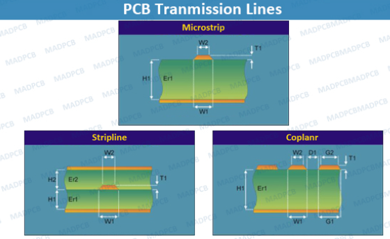
(3) RF/Microwave Signal Lines
High-frequency signals (MHz to GHz range) used in wireless communication.
Key Characteristics:
- Requires precise impedance control (50Ω or 75Ω).
- Microstrip or stripline routing techniques.
- Sensitive to parasitic capacitance/inductance.
Applications:
- Antenna feeds
- WiFi/Bluetooth modules
- Radar systems
4. Classification Based on Power Delivery
(1) Power Traces
Carry supply voltage to components.
Key Characteristics:
- Wider traces to reduce resistance and voltage drop.
- May require multiple vias for current handling.
Applications:
- Voltage regulator outputs
- Power distribution networks
(2) Ground Traces
Provide return paths for signals and power.
Key Characteristics:
- Should form low-impedance paths.
- Critical for EMI control.
Applications:
- Ground planes in multilayer PCBs
(3) Signal Return Paths
The path through which signal currents flow back to the source.
Key Characteristics:
- Should be as close as possible to the signal trace.
- Discontinuities can cause EMI and signal integrity issues.
Applications:
- High-speed digital circuits
5. Key Differences Between Signal Line Types
| Feature | Analog Signals | Digital Signals | Differential Pairs | RF Signals |
|---|---|---|---|---|
| Noise Immunity | Low | Moderate | High | High |
| Routing Complexity | Moderate | Low to High | High | Very High |
| Impedance Control | Sometimes | Critical for HS | Critical | Mandatory |
| Typical Applications | Sensors, Audio | Processors, Memory | USB, Ethernet | WiFi, 5G |
Conclusion
PCB signal lines vary significantly based on their function, transmission properties, and frequency requirements. Proper classification helps in designing optimized layouts for signal integrity, noise immunity, and EMI compliance. High-speed and RF signals demand controlled impedance and careful routing, while analog signals require isolation from noise sources. Differential signaling enhances noise rejection in high-speed applications. By understanding these classifications, engineers can design efficient and reliable PCBs for diverse electronic systems.
Future trends, such as higher data rates in 5G and AI hardware, will further emphasize the importance of advanced signal line design techniques.