CNC PCB Milling: A Comprehensive Guide
Introduction
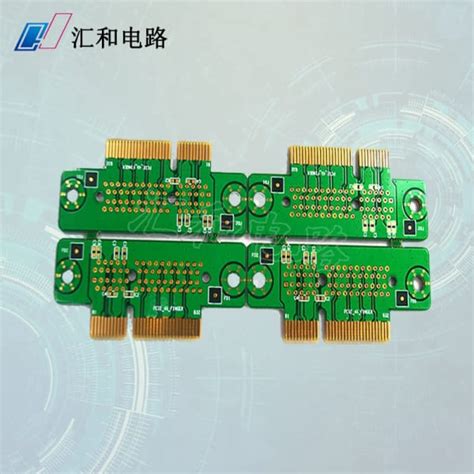
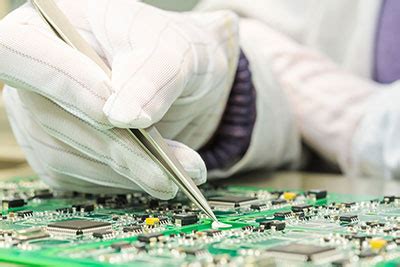
Printed Circuit Boards (PCBs) are essential components in modern electronics, serving as the foundation for connecting and supporting electronic components. While traditional PCB manufacturing involves chemical etching, CNC PCB milling has emerged as a fast, precise, and environmentally friendly alternative. This method uses Computer Numerical Control (CNC) machines to mechanically remove copper from a substrate, creating conductive traces and isolation paths.
This article explores CNC PCB milling, covering its principles, advantages, limitations, workflow, and applications. By the end, you’ll understand why this technique is popular among hobbyists, engineers, and small-scale manufacturers.
1. What is CNC PCB Milling?
CNC PCB milling is a subtractive manufacturing process where a rotating cutting tool (end mill) removes unwanted copper from a PCB substrate to form circuits. Unlike chemical etching, which uses corrosive chemicals, milling is a cleaner, more controlled method.
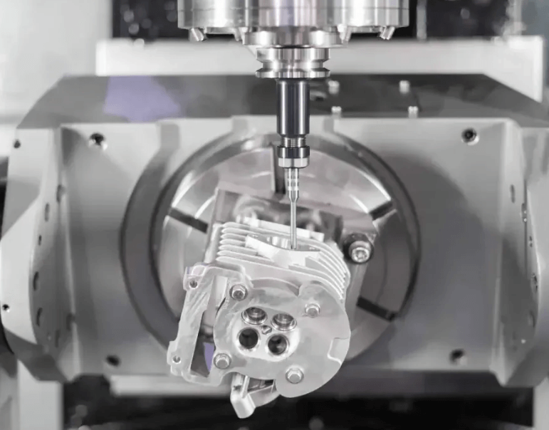
Key Components of a CNC PCB Milling Machine
- Spindle: Rotates the cutting tool at high speeds (typically 10,000–60,000 RPM).
- End Mills (Bits): Small drill bits (0.1–3.0 mm) that carve out traces.
- Motion Control System: Uses stepper/servo motors to move the spindle along X, Y, and Z axes.
- Workbed: A flat surface where the PCB is secured.
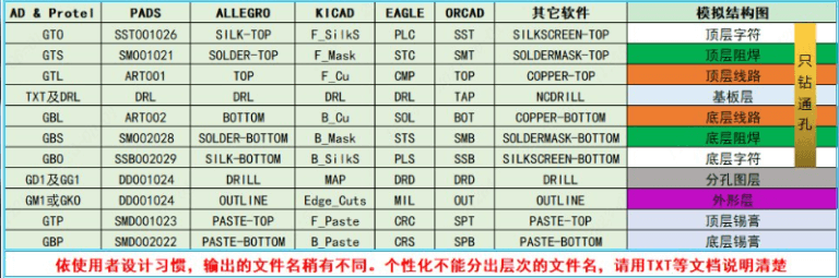
- Software: Converts PCB designs (Gerber files) into machine instructions (G-code).
2. Advantages of CNC PCB Milling
2.1 Rapid Prototyping
- Unlike traditional PCB fabrication (which takes days), milling allows same-day prototyping.
- Ideal for iterative design processes.
2.2 No Chemicals Required
- Eliminates hazardous etchants like ferric chloride.
- Safer for home labs and educational environments.
2.3 High Precision
- Achieves trace widths as small as 0.1 mm (depending on the machine).
- Suitable for high-frequency and RF circuits where precision is critical.
2.4 Flexibility in Design Changes
- Modifications can be made on-the-fly without waiting for new boards.
- Allows single-sided, double-sided, and even multilayer PCBs (with advanced setups).
2.5 Cost-Effective for Small Batches
- Avoids high setup costs associated with commercial PCB production.
- No minimum order quantity—ideal for custom projects.
3. Limitations of CNC PCB Milling
3.1 Slower for Large Production Runs
- Milling is not scalable for mass production (chemical etching or outsourcing is better for large quantities).
3.2 Limited to Simple Designs
- Very fine-pitch components (e.g., BGA, QFN) may be challenging due to bit size limitations.
- Via drilling and plating require additional steps.
3.3 Tool Wear
- Small end mills wear out quickly, requiring frequent replacement.
- Poor tool life when milling fiberglass (FR4) PCBs.
3.4 Surface Finish Quality
- Milled traces may have rough edges, requiring manual cleanup.
- Not as smooth as chemically etched or professionally manufactured PCBs.
4. CNC PCB Milling Workflow
4.1 Design the PCB
- Use PCB design software (KiCad, Eagle, Altium).
- Export Gerber and drill files.
4.2 Generate Toolpaths
- Convert Gerber files to G-code using FlatCAM, Bantam Tools, or OpenBuilds.
- Define:
- Trace isolation paths (removing copper around traces).
- Drill holes (for through-hole components).
- Board outline cutting.
4.3 Secure the PCB Blank
- Clamp or vacuum-secure a copper-clad board to the workbed.
- Ensure proper leveling to avoid uneven milling.
4.4 Machine Setup
- Install the correct end mill (V-bit for traces, drill bit for holes).
- Set spindle speed, feed rate, and depth per pass (optimized for copper and substrate material).
4.5 Run the Milling Job
- Execute the G-code.
- Monitor for tool breakage or misalignment.
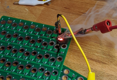
4.6 Post-Processing
- Deburring: Remove rough edges with fine sandpaper.
- Cleaning: Wash away copper dust.
- Soldering: Populate components.
5. Applications of CNC PCB Milling
5.1 Prototyping & R&D
- Engineers use milling for quick design validation before mass production.
5.2 Education & DIY Electronics
- Universities and makerspaces use CNC mills for hands-on PCB fabrication training.
5.3 Custom & Low-Volume PCBs
- Ideal for specialized industrial controls, robotics, and IoT devices.
5.4 RF & High-Frequency Circuits
- Milling allows precise impedance control for RF applications.
5.5 Repair & Modification
- Enables trace repairs on damaged PCBs.
6. Choosing the Right CNC Machine for PCB Milling
6.1 Desktop CNC Mills
- Bantam Tools Desktop PCB Milling Machine: High precision, user-friendly.
- Roland MonoFab SRM-20: Reliable for small PCBs.
- OpenBuilds Workbee: Affordable DIY option.
6.2 Industrial-Grade Machines
- LPKF ProtoMat: Professional-grade, supports multilayer PCBs.
- T-Tech Quick Circuit: High-speed, automated milling.
6.3 Key Considerations
- Spindle Speed: ≥ 30,000 RPM for clean cuts.
- Resolution: At least 0.01 mm positioning accuracy.
- Software Compatibility: Ensure support for standard PCB file formats.
7. Future Trends in CNC PCB Milling
- Hybrid Machines: Combining milling with laser etching for finer traces.
- Automated Tool Changers: Reducing manual intervention.
- AI-Based Optimization: Smart G-code generation for better efficiency.
- Integration with 3D Printing: For fully assembled PCBs in one machine.
Conclusion
CNC PCB milling is a versatile, fast, and eco-friendly alternative to traditional PCB fabrication. While it has limitations in mass production, it excels in prototyping, education, and custom electronics. As CNC technology advances, milling will become even more accessible and precise, further empowering engineers and makers.
Whether you’re a hobbyist, student, or professional, CNC PCB milling offers a hands-on, efficient way to bring your electronic designs to life.