Common Causes of SMT Welding Defects: A Comprehensive Analysis
Surface Mount Technology (SMT) has revolutionized the electronics manufacturing industry by enabling the production of smaller, faster, and more reliable electronic devices. However, the SMT welding process is complex and prone to various defects that can compromise the quality and reliability of the final product. Understanding the common causes of SMT welding defects is essential for improving manufacturing processes, reducing costs, and ensuring product reliability. This article provides a comprehensive analysis of the primary causes of SMT welding defects, including material, process, design, and environmental factors.
1. Introduction to SMT Welding Defects
SMT welding defects occur when the solder joints between surface-mount components and the PCB are compromised, leading to electrical or mechanical failure. These defects can manifest as incomplete solder joints, solder bridges, tombstoning, or voids. SMT welding defects are particularly problematic in high-reliability applications, such as aerospace, automotive, and medical devices, where even a single defect can have severe consequences.
2. Common SMT Welding Defects and Their Causes
2.1 Solder Bridging
Solder bridging occurs when solder connects adjacent pads or pins, causing a short circuit.
Causes:
- Excessive Solder Paste: Applying too much solder paste can cause it to spread and form bridges between adjacent pads.
- Incorrect Stencil Aperture Design: Poorly designed stencil apertures can lead to excessive solder paste deposition.
- Component Misalignment: Misaligned components can cause solder paste to spread and form bridges.
- Insufficient Solder Mask: Inadequate solder mask between pads can allow solder to flow and create bridges.
2.2 Tombstoning
Tombstoning occurs when one end of a surface-mount component lifts off the pad during reflow, resulting in an open circuit.
Causes:
- Uneven Heating: Uneven heating during reflow can cause one end of the component to melt and lift before the other.
- Incorrect Pad Design: Pads that are too large or too small can cause uneven solder wetting and lead to tombstoning.
- Component Size Mismatch: Using components that are too small or too large for the pads can cause uneven solder distribution.
- Insufficient Solder Paste: Insufficient solder paste on one pad can cause uneven wetting and lead to tombstoning.
2.3 Insufficient Solder (Cold Joints)
Insufficient solder results in weak or incomplete solder joints, leading to poor electrical connections.
Causes:
- Insufficient Solder Paste: Applying too little solder paste can result in incomplete solder joint formation.
- Incorrect Reflow Profile: An improperly designed reflow profile can cause the solder to not fully melt and wet the surfaces.
- Poor Wetting: Contaminated or oxidized surfaces can prevent proper solder wetting, leading to incomplete joints.
- Incorrect Stencil Aperture Design: Poorly designed stencil apertures can lead to insufficient solder paste deposition.
2.4 Solder Balls
Solder balls are small spheres of solder that form on the PCB surface, potentially causing short circuits.
Causes:
- Excessive Solder Paste: Applying too much solder paste can cause it to splatter and form solder balls during reflow.
- Incorrect Reflow Profile: An improperly designed reflow profile can cause solder paste to splatter and form solder balls.
- Contaminated Solder Paste: Contaminants in the solder paste can cause it to splatter and form solder balls.
- Insufficient Solder Mask: Inadequate solder mask can allow solder to flow and form balls.
2.5 Voids
Voids are air pockets within the solder joint that can weaken the joint and reduce thermal conductivity.
Causes:
- Outgassing: Volatile compounds in the solder paste or PCB can outgas during reflow, creating voids.
- Incorrect Reflow Profile: An improperly designed reflow profile can cause incomplete outgassing, leading to voids.
- Poor Solder Paste Application: Inconsistent or improper solder paste application can lead to voids.
- Contaminated Surfaces: Contaminated or oxidized surfaces can prevent proper solder wetting, leading to voids.
2.6 Component Misalignment
Component misalignment occurs when surface-mount components are not properly placed on their pads, leading to poor solder joints.
Causes:
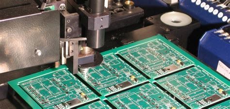
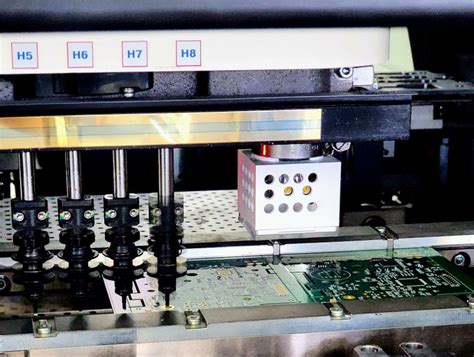
- Pick-and-Place Machine Calibration: Improper calibration of the pick-and-place machine can cause misalignment.
- Incorrect Pad Design: Pads that are too large or too small can cause components to shift during reflow.
- Insufficient Adhesive: Insufficient adhesive to hold components in place during reflow can cause misalignment.
- Vibration or Movement: Vibration or movement during the reflow process can cause components to shift.
2.7 Solder Cracking
Solder cracking occurs when the solder joint fractures, leading to an open circuit.
Causes:
- Thermal Cycling: Repeated temperature changes can cause mechanical stress in solder joints, leading to cracking.
- Mechanical Stress: Vibration or shock can cause solder joints to crack.
- CTE Mismatch: Differences in the coefficient of thermal expansion (CTE) between the PCB, components, and solder alloy can cause stress and cracking.
- Poor Solder Joint Formation: Weak or incomplete solder joints are more prone to cracking.

3. Best Practices for Preventing SMT Welding Defects
3.1 Material Selection
- Choose High-Quality Solder Paste: Use solder paste with appropriate alloy composition and flux properties.
- Ensure Clean Surfaces: Ensure that PCB pads and component leads are clean and free of oxidation or contamination.
3.2 Process Optimization
- Control Solder Paste Application: Use precise stencil design and application techniques to ensure consistent solder paste deposition.
- Optimize Reflow Profile: Design the reflow profile to ensure proper solder melting and wetting.
- Calibrate Pick-and-Place Machines: Ensure that pick-and-place machines are properly calibrated to achieve accurate component placement.
3.3 Design Improvements
- Optimize Pad and Stencil Design: Ensure that pads and stencil apertures are properly sized and shaped to support strong solder joints.
- Use Adequate Solder Mask: Ensure sufficient solder mask between pads to prevent solder bridging.
- Consider Thermal Management: Design for effective heat dissipation and minimize CTE mismatch between materials.
3.4 Environmental Protection
- Control Manufacturing Environment: Maintain a clean and controlled manufacturing environment to prevent contamination.
- Use Conformal Coatings: Apply conformal coatings to protect solder joints from moisture, dust, and contaminants.
3.5 Testing and Inspection
- Conduct Automated Optical Inspection (AOI): Use AOI to detect defects such as insufficient solder, bridging, or misalignment.
- Perform X-Ray Inspection: Use X-ray inspection to identify hidden defects, such as voids or cracks in solder joints.
- Conduct Thermal Cycling Tests: Test the PCB under thermal cycling conditions to identify potential solder joint failures.
4. Emerging Trends in SMT Welding Quality
4.1 Advanced Solder Alloys
- Nanocomposite Solders: Incorporating nanoparticles into solder alloys to improve mechanical and thermal properties.
- Low-Temperature Solders: Developing solder alloys with lower melting points to reduce thermal stress during assembly.
4.2 Additive Manufacturing
- 3D Printing of Solder Joints: Using additive manufacturing techniques to create customized solder joint geometries for improved reliability.
4.3 Smart Manufacturing
- Real-Time Process Monitoring: Using IoT and data analytics to monitor and optimize soldering processes in real time.
- Predictive Maintenance: Implementing predictive maintenance strategies to identify and address potential solder joint failures before they occur.
5. Conclusion
SMT welding defects can result from a wide range of factors, including material selection, process control, design considerations, and environmental conditions. By understanding these causes and implementing best practices for prevention, manufacturers can improve the reliability and performance of their SMT assemblies. Emerging trends, such as advanced solder alloys, additive manufacturing, and smart manufacturing, offer new opportunities for enhancing SMT welding quality and reducing the risk of defects. With careful attention to detail and adherence to industry standards, SMT welding defects can be minimized, ensuring the long-term success of electronic products.


