Common drilling problems when drawing PCB boards
The design of electronic products is from drawing schematics to PCB layout and wiring. Due to lack of work experience and knowledge, various errors often occur, which hinder our subsequent work. In serious cases, the circuit boards produced cannot be used at all. Therefore, we must try our best to improve our knowledge in this area to avoid various errors.
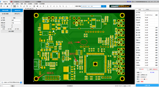
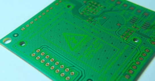
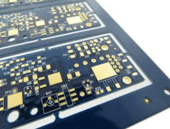
This article introduces common drilling problems when drawing PCB boards to avoid stepping on the same pit in the future. Drilling is divided into three categories: through holes, blind holes, and buried holes. Through holes include plug-in holes (PTH) and screw positioning holes (NPTH). Blind, buried and through-hole vias (VIA) all play the role of multi-layer electrical conduction. Regardless of the type of hole, the consequence of the missing hole is that the entire batch of products cannot be used directly. Therefore, the correctness of the drilling design is particularly important.
Case explanation
Problem 1: The file slot designed by Altium is placed on the wrong layer;
Problem description: The slot is missed and the product cannot be used.
Cause analysis: The design engineer missed the slot of the USB device when making the package. When the problem was found in the drawing board, the package was not modified, and the slot was directly drawn on the hole symbol layer. In theory, this operation is not a big problem, but in the manufacturing process, only the drilling layer is used for drilling, so it is easy to ignore the existence of slots in other layers, resulting in the slot being missed and the product cannot be used. Please see the figure below;
How to avoid the pit: Each layer of the PCB design file has its own function. Drilling and slots must be placed on the drilling layer. It cannot be assumed that the design can be manufactured.
Problem 2: Altium design file via 0 D code;
Problem description: The leaked via is open and not conductive.
Cause analysis: Please see Figure 1. There is a leak in the design file. When performing DFM manufacturability inspection, a leak is prompted. After checking the cause of the leak, the aperture size of the leak is 0 in the Altium software, resulting in no holes in the design file, see Figure 2.
The cause of this leak is the design engineer’s mistaken operation when punching. If the problem of this leak is not checked, it is difficult to find that there is a leak in the design file. The leak directly affects the electrical conduction and the designed product cannot be used.
How to avoid pitfalls: DFM manufacturability testing must be performed after the circuit diagram design is completed. Leakage during design cannot be found in manufacturing and production. DFM manufacturability testing before manufacturing can avoid this problem.
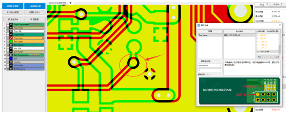
Figure 1: Design file leak
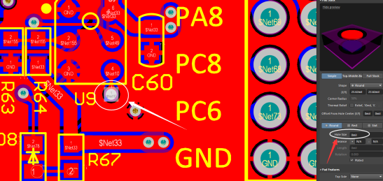
Figure 2: Altium aperture is 0
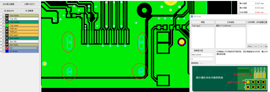
Problem 3: The vias in the PADS design file cannot be output;
Problem description: The leaked vias are open and non-conductive.
Cause analysis: Please see Figure 1. When using DFM manufacturability detection, many leaks are prompted. After checking the cause of the leak problem, one group of vias in PADS is designed as semi-conducting vias, resulting in the design file not outputting semi-conducting vias, resulting in leaks. Please see Figure 2.
There are no semi-conducting vias on the double-sided board. The engineer mistakenly set the vias as semi-conducting vias during the design. When outputting the drilling, the semi-conducting vias were not output, resulting in leaks.
How to avoid pitfalls: This type of misoperation is not easy to find. After the design is completed, DFM manufacturability analysis and inspection are required to find problems before manufacturing to avoid leaks.
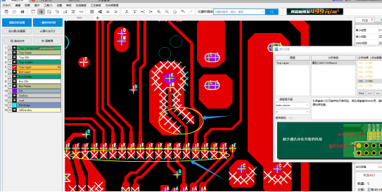
Figure 1: Design file leaks
Figure 2: PADS software double-sided board vias are semi-conducting holes
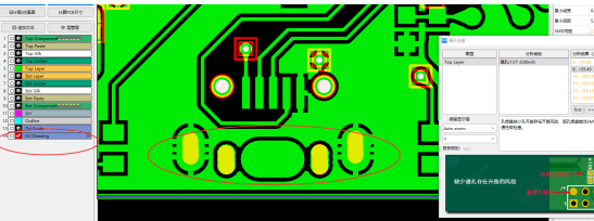
Problem 4: Allegro’s Gerber file leaks slots;
Problem description: HDMI device leaks pin holes and cannot be plugged in.
Cause analysis: Please see Figure 1, and the leak is prompted when using DFM manufacturability inspection. After checking the cause of the leak problem, the output Gerber file lacks slot hole layers. The reason for the leak of slot hole layers is that the output drilling is not continued, resulting in the leak of slot holes. Please see Figure 2.
If the pin of a HDMI device leaks a slot, the device pin cannot be inserted. This pin generally has a ground network. If the multilayer board is drilled again, the ground network will be open.
How to avoid pitfalls: For novices, it is easy to forget the output slot layer. Therefore, DFM must be used for manufacturability inspection before plate making to avoid the problem of leaking slot holes.

Figure 1: Leaking slot holes
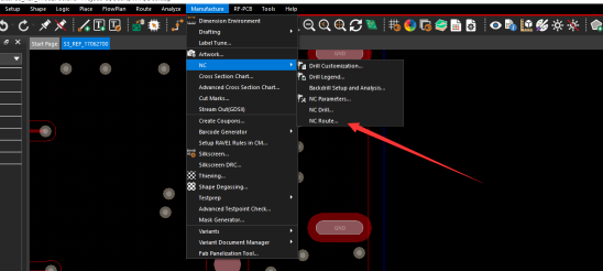
Figure 2: Output ROU layer
The holes in the PCB circuit board design are very important. The routing needs to be drilled through the hole, the structure needs to be drilled with a positioning hole, and the DIP device needs to be drilled with a plug-in hole. If the design leaks holes, the design will fail.