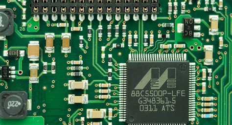
Common Issues in PCB Prototyping and How to Avoid Them
Printed Circuit Board (PCB) prototyping is a critical phase in electronics development, allowing engineers to test designs before mass production. However, PCB prototype manufacturing is prone to various issues that can lead to delays, increased costs, or even complete board failures. This article explores the most common problems encountered in PCB prototyping and provides practical solutions to mitigate them.

1. Design Errors Leading to Manufacturing Defects
Problem:
Many PCB prototype failures stem from design mistakes, such as incorrect trace widths, improper spacing, or flawed component footprints. Common issues include:
- Insufficient Clearance: Traces or pads placed too close together can cause short circuits.
- Incorrect Layer Stackup: Poorly defined layer ordering or dielectric materials can affect signal integrity.
- Missing or Wrong Drill Holes: Misaligned or missing vias and through-holes prevent proper component mounting.
Solution:
- Use Design Rule Checks (DRC) and Electrical Rule Checks (ERC) in CAD tools (e.g., Altium, KiCad, Eagle).
- Verify footprint accuracy by cross-referencing datasheets.
- Simulate signal integrity with tools like HyperLynx or SPICE models.
2. Poor Solder Mask Application
Problem:
Solder mask defects can cause bridging, corrosion, or poor solder joints. Issues include:
- Misalignment: Exposing unintended copper areas.
- Incomplete Coverage: Leaving traces vulnerable to oxidation.
- Bubbling or Peeling: Due to improper curing or low-quality materials.
Solution:
- Ensure solder mask expansion settings are correct (typically 0.05mm–0.1mm beyond pads).
- Specify solder mask thickness (usually 10–25µm).
- Use high-quality UV-curable solder mask materials.
3. Incorrect PCB Material Selection
Problem:
Choosing the wrong substrate can lead to thermal, mechanical, or electrical failures:
- FR-4 vs. High-Frequency Materials: FR-4 is standard but unsuitable for RF/microwave applications.
- Thermal Expansion Mismatch: Causes warping or delamination under thermal stress.
- Poor Dielectric Properties: Leading to signal loss or crosstalk.
Solution:
- For high-frequency PCBs, use Rogers, PTFE, or ceramic-filled materials.
- For high-temperature applications, consider polyimide or aluminum-backed PCBs.
- Verify glass transition temperature (Tg) and coefficient of thermal expansion (CTE).
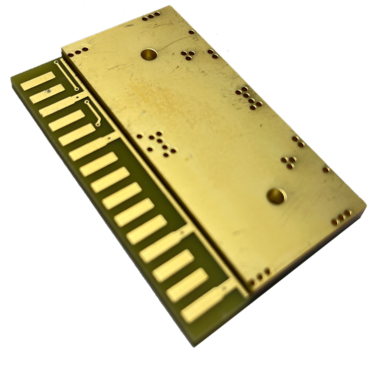
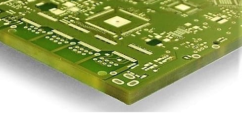
4. Via and Plating Defects
Problem:
Vias are critical for multilayer PCBs but often suffer from:
- Incomplete Plating: Leading to open circuits.
- Microvoids: Causing weak electrical connections.
- Barrel Cracks: Due to thermal stress or mechanical drilling issues.
Solution:
- Use tented vias to prevent solder wicking.
- Specify copper thickness (standard: 1oz, high-current: 2–3oz).
- For HDI designs, consider laser-drilled microvias.
5. Silkscreen Errors
Problem:
Silkscreen misprints may not affect functionality but can cause assembly errors:
- Faded or Smudged Text: Making component labels unreadable.
- Incorrect Polarity Markings: Leading to reversed component placement.
- Overlapping Pads: Obstructing solder paste application.
Solution:
- Use legible fonts (e.g., Arial, Verdana) with a minimum line width of 0.15mm.
- Keep silkscreen ≥0.2mm away from pads.
- Double-check polarity indicators (e.g., “+,” “-,” pin 1 markers).
6. Inadequate Testing and Quality Control
Problem:
Many prototype failures occur due to skipped testing steps:
- No Electrical Testing (ET): Missing open/short circuits.
- Insufficient Functional Testing: Undetected design flaws.
- Poor DFM (Design for Manufacturability) Checks: Leading to unmanufacturable designs.
Solution:
- Perform Automated Optical Inspection (AOI) and Flying Probe Testing.
- Use boundary scan (JTAG) for complex boards.
- Partner with manufacturers offering DFM feedback before production.
7. Environmental and Handling Damage
Problem:
Prototypes are often mishandled, leading to:
- ESD (Electrostatic Discharge) Damage: Killing sensitive ICs.
- Moisture Absorption: Causing delamination during reflow.
- Mechanical Stress: Cracking brittle components.
Solution:
- Store PCBs in anti-static bags with desiccants.
- Follow IPC handling guidelines for moisture-sensitive devices (MSD).
- Use protective packaging during shipping.
Conclusion
PCB prototyping is prone to errors, but most issues can be avoided with careful design, material selection, and thorough testing. By addressing common pitfalls—such as design flaws, solder mask defects, via failures, and inadequate testing—engineers can improve prototype success rates and accelerate product development.
Best Practices Summary:
✔ Always run DRC/ERC before fabrication.
✔ Verify solder mask and silkscreen alignment.
✔ Choose appropriate materials for the application.
✔ Perform electrical and functional testing.
✔ Handle prototypes with ESD and moisture protection.
By following these guidelines, PCB prototype failures can be significantly reduced, saving time and costs in the development cycle.