Common PCB Design Mistakes and How to Solve Them
Printed Circuit Board (PCB) design is a complex process that requires careful attention to detail. Even experienced designers can make mistakes that lead to manufacturing issues, reduced performance, or complete board failures. This article explores the most common PCB design errors and provides practical solutions to avoid or fix them.
1. Incorrect Component Footprints
One of the most frequent and costly mistakes in PCB design is using incorrect component footprints.
Common Issues:
- Pad sizes that don’t match component leads
- Wrong pin spacing or count
- Inaccurate 3D dimensions causing mechanical interference
- Incorrect polarity markings
Solutions:
- Double-check datasheets: Always verify dimensions from the manufacturer’s latest datasheet
- Create a library system: Maintain a verified component library with version control
- Use 3D models: Visual verification can catch mechanical conflicts
- Print 1:1 scale: Physical comparison with components before production
- Prototype testing: Order a small batch for verification before full production

2. Poor Power Distribution Network Design
Power integrity issues can lead to unstable operation and mysterious failures.
Common Issues:
- Inadequate decoupling capacitor placement
- Thin power traces causing voltage drops
- Improper power plane segmentation
- Lack of proper current capacity analysis
Solutions:
- Follow the 20H rule: Keep power planes smaller than ground planes to reduce edge radiation
- Proper decoupling: Place capacitors close to power pins (high-frequency caps nearest)
- Wide traces: Calculate trace widths based on current requirements
- Multiple vias: Use several vias for high-current connections
- Simulation tools: Use power integrity simulation before manufacturing
3. Signal Integrity Problems
With increasing clock speeds, signal integrity has become critical in PCB design.
Common Issues:
- Impedance mismatches
- Excessive trace lengths
- Poor return paths
- Crosstalk between signals
- Reflections due to improper termination
Solutions:
- Controlled impedance routing: Match trace geometry to required impedance
- Proper layer stackup: Ensure adjacent reference planes for high-speed signals
- Length matching: For differential pairs and timing-critical signals
- Adequate spacing: Follow 3W rule (trace spacing ≥ 3× trace width) for sensitive signals
- Termination resistors: Use appropriate termination for transmission lines
4. Thermal Management Issues
Overheating components can reduce reliability and lifespan of the PCB.
Common Issues:
- Insufficient copper for heat dissipation
- Poor component placement creating hot spots
- Lack of thermal vias under heat-generating components
- Inadequate airflow consideration
Solutions:
- Thermal relief pads: Use them appropriately (not for power components)
- Copper pours: Add extra copper for heat dissipation
- Thermal vias: Place under hot components to transfer heat to other layers
- Simulation: Perform thermal analysis before production
- Component spacing: Allow adequate space around heat-generating parts
5. Manufacturing Design Rule Violations
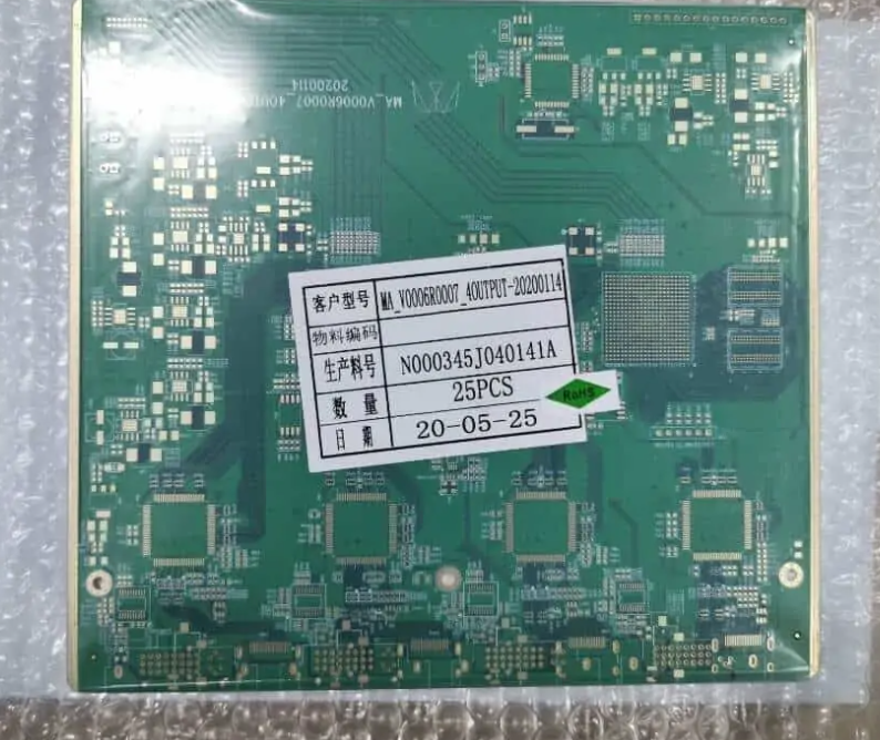
Designs that don’t account for manufacturing capabilities can lead to production issues.
Common Issues:
- Traces too close to board edges
- Insufficient annular ring for vias
- Drill sizes too small for manufacturer’s capabilities
- Silkscreen over pads
- Inadequate solder mask clearance
Solutions:
- Know your manufacturer’s capabilities: Obtain and follow their design rules
- Design rule check (DRC): Run comprehensive DRC before finalizing
- Adequate clearances: Follow IPC standards for spacing
- Test points: Include accessible test points for manufacturing testing
- Panelization considerations: Account for breakaway tabs and routing if panelizing
6. Poor Grounding Practices
Grounding issues are among the most common causes of noise and interference problems.
Common Issues:
- Ground loops
- Split ground planes creating return path issues
- Insufficient ground connections
- Mixed analog and digital grounds without proper separation
Solutions:
- Single-point grounding: For low-frequency circuits to avoid ground loops
- Solid ground plane: Preferred for most designs
- Proper partitioning: If splitting grounds, do it at one point only
- Multiple vias: Connect ground layers with many vias
- Star grounding: For sensitive analog circuits
7. Inadequate DFM (Design for Manufacturing) Considerations
Designs that aren’t optimized for manufacturing can increase costs and reduce yield.
Common Issues:
- Unnecessary small vias and traces
- Components too close for automated assembly
- Lack of fiducial marks
- Improper component orientation for wave soldering
- Missing solder mask between fine-pitch components
Solutions:
- Follow DFM guidelines: Understand SMT and through-hole assembly requirements
- Component spacing: Follow IPC-7351 standards
- Fiducial marks: Include global and local fiducials for pick-and-place machines
- Assembly drawing: Provide clear documentation for manufacturers
- Testability: Consider how the board will be tested during manufacturing
8. Insufficient Testing Considerations
Failing to design for testability can make debugging and production testing difficult.
Common Issues:
- No test points for critical signals
- Components blocking access to test points
- Lack of built-in self-test features
- No programming/debugging interface
Solutions:
- Add test points: For all important signals and power rails
- Boundary scan: Consider IEEE 1149.1 (JTAG) for complex boards
- Test access: Ensure probe points are accessible
- Design for debugging: Include LEDs, headers, or other diagnostic aids
- In-circuit test (ICT): Design with ICT requirements if used
9. Documentation Errors
Poor documentation can lead to assembly mistakes and debugging challenges.
Common Issues:
- Missing or incorrect BOM (Bill of Materials)
- Wrong component designators on silkscreen
- Incomplete assembly drawings
- Missing revision control
Solutions:
- Automated BOM generation: Extract from design software
- Silkscreen review: Verify all component designators are visible
- Complete documentation package: Include assembly drawings, schematics, layer plots
- Revision control: Clearly mark and track design revisions
- 3D PDF: Provide 3D visualization for mechanical verification
10. EMC/EMI Problems
Electromagnetic compatibility issues can cause products to fail regulatory testing.
Common Issues:
- Poor filtering of I/O lines
- Inadequate shielding
- Clock signals radiating excessive EMI
- Improper cable grounding
Solutions:
- Proper filtering: Add ferrites and filters to I/O lines
- Shielding: Consider shielded enclosures or board-level shields
- Clock routing: Keep clock traces short and away from board edges
- Grounding: Ensure proper cable shield grounding
- Pre-compliance testing: Test EMC performance before formal certification
Best Practices to Avoid Common PCB Errors
- Use a Checklist: Develop and follow a comprehensive pre-production checklist
- Peer Review: Have another engineer review your design
- Design Rules: Set up and use design rule checking in your EDA software
- Prototype: Always build and test prototypes before full production
- Continuous Learning: Stay updated on new technologies and design techniques
- Library Management: Maintain a well-organized, verified component library
- Manufacturer Collaboration: Communicate with your PCB fabricator early in the design process
Conclusion
PCB design errors can be costly and time-consuming to fix, especially when discovered after production. By understanding these common mistakes and implementing the suggested solutions, designers can significantly improve their PCB design quality and reliability. Remember that prevention is always better than correction—investing time in careful design and verification upfront will save considerable time and resources later in the product development cycle.
As PCB technology continues to advance with higher densities and faster signals, the importance of proper design practices only increases. By combining knowledge of these common pitfalls with modern design tools and verification methods, engineers can produce robust, reliable PCBs that meet all performance and manufacturing requirements.

