Common PCB Inspection Techniques and Equipment: A Comprehensive Guide
Introduction
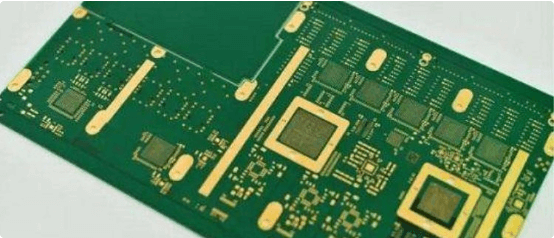
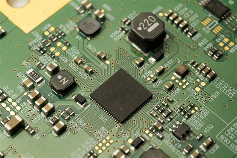
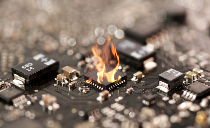
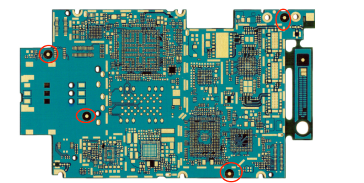
Printed Circuit Boards (PCBs) are the backbone of modern electronics, found in everything from smartphones to industrial machinery. Ensuring their quality and reliability is crucial, as even minor defects can lead to system failures. To maintain high manufacturing standards, various PCB inspection techniques and equipment are employed at different stages of production.
This article explores the most common PCB inspection methods, including manual inspection, automated optical inspection (AOI), X-ray inspection, and electrical testing. We will also discuss the equipment used in these processes and their advantages and limitations.
1. Manual Visual Inspection (MVI)
Overview
Manual Visual Inspection (MVI) is one of the oldest and simplest PCB inspection methods. It involves human operators examining PCBs under magnification to detect visible defects such as soldering issues, misaligned components, or damaged traces.
Equipment Used
- Magnifying Lenses & Microscopes – Used for close-up examination.
- Lighting Systems – Proper illumination helps in identifying defects.
- Inspection Jigs – Hold PCBs in place for consistent viewing angles.
Advantages
- Low-cost and easy to implement.
- Effective for small-scale production or prototypes.
Limitations
- Prone to human error and fatigue.
- Time-consuming for large batches.
- Limited to surface-level defects.

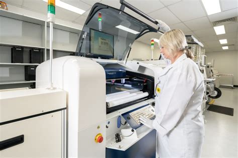
2. Automated Optical Inspection (AOI)
Overview
Automated Optical Inspection (AOI) uses high-resolution cameras and image processing software to detect defects on PCBs. It is widely used in surface-mount technology (SMT) assembly lines.
Equipment Used
- High-Resolution Cameras – Capture detailed images of PCBs.
- LED Lighting Systems – Enhance visibility of solder joints and components.
- Image Processing Software – Compares captured images with reference designs to identify discrepancies.
Common Defects Detected
- Solder bridges
- Missing or misaligned components
- Incorrect polarity
- Scratches or cracks
Advantages
- Fast and consistent inspection.
- Suitable for high-volume production.
- Can detect a wide range of defects.
Limitations
- Cannot inspect hidden solder joints (e.g., under BGA components).
- Requires proper programming and calibration.
3. X-Ray Inspection (AXI)
Overview
X-ray inspection is used to examine hidden solder joints, such as those in Ball Grid Array (BGA) and Quad Flat No-leads (QFN) packages. It provides a non-destructive way to inspect internal structures.
Equipment Used
- X-Ray Imaging Systems – Generate high-resolution cross-sectional images.
- Computed Tomography (CT) Scanners – Provide 3D views of PCB layers.
- Automated Analysis Software – Detects voids, cracks, and insufficient solder.
Common Defects Detected
- Solder voids
- Insufficient or excessive solder
- Cracked joints
- Misaligned BGA balls
Advantages
- Capable of inspecting hidden solder joints.
- Non-destructive testing method.
- Provides detailed internal images.
Limitations
- Expensive equipment and maintenance.
- Requires skilled operators.
- Slower than AOI for large-scale inspections.
4. In-Circuit Testing (ICT)
Overview
In-Circuit Testing (ICT) is an electrical testing method that checks the functionality of individual components on a PCB. It uses a bed-of-nails fixture to make contact with test points.
Equipment Used
- Bed-of-Nails Fixture – Contains multiple spring-loaded pins for electrical contact.
- Automated Test Equipment (ATE) – Measures resistance, capacitance, and voltage.
- Test Software – Compares measurements against expected values.
Common Tests Performed
- Shorts and opens detection.
- Component value verification (resistors, capacitors).
- Diode and transistor functionality.
Advantages
- Highly accurate for detecting electrical faults.
- Can test multiple components simultaneously.
- Suitable for high-volume production.
Limitations
- Requires custom fixtures for different PCB designs.
- Limited to accessible test points.
- Not effective for detecting mechanical defects.
5. Flying Probe Testing
Overview
Flying Probe Testing is a non-fixture-based electrical testing method that uses movable probes to check PCB functionality. It is ideal for low-volume or prototype testing.
Equipment Used
- Robotic Probes – Move dynamically to test different points.
- Precision Motion Control System – Ensures accurate probe positioning.
- High-Speed Test Software – Analyzes electrical parameters.
Advantages
- No need for custom fixtures.
- Flexible for design changes.
- Suitable for complex PCBs.
Limitations
- Slower than ICT for large batches.
- Higher operational cost compared to ICT.
6. Functional Testing (FCT)
Overview
Functional Testing (FCT) verifies that the PCB operates as intended in its final application. It simulates real-world conditions to ensure performance.
Equipment Used
- Test Fixtures & Interfaces – Connects the PCB to test equipment.
- Signal Generators & Analyzers – Simulate input/output conditions.
- Software Scripts – Automate test sequences.
Common Tests Performed
- Power-up and boot sequence verification.
- Signal integrity testing.
- Firmware and software validation.
Advantages
- Ensures end-product functionality.
- Detects system-level issues.
Limitations
- Requires custom test setups.
- May not identify root causes of defects.
Conclusion
PCB inspection is a critical step in ensuring product reliability. From manual visual checks to advanced X-ray and electrical testing, each method has its strengths and limitations. Manufacturers often combine multiple techniques to achieve comprehensive quality control.
As PCB technology evolves with finer pitches and higher component density, inspection methods will continue to advance, incorporating AI and machine learning for even greater accuracy and efficiency.
By understanding these common PCB inspection techniques and equipment, manufacturers can optimize their quality assurance processes and deliver defect-free electronic products.