Compact Slingshot PCB Assembly Strategies for Rugged Device Integration

Key Takeaways
Effective PCB assembly (PCBA) for rugged devices demands specialized strategies to ensure durability in harsh operating conditions. Prioritizing shockproof layouts involves strategic placement of stress-sensitive components away from high-impact zones, complemented by reinforced anchoring points. Implementing vibration-resistant soldering techniques—such as underfill encapsulation or corner bonding—enhances joint integrity under mechanical stress.
Tip: When designing for vibration resistance, consider using flexible adhesives in conjunction with traditional soldering to absorb harmonic oscillations without compromising electrical connections.
Component stacking optimization requires balancing spatial efficiency with thermal management, often achieved through 3D modeling to predict stress distribution. Ruggedized PCBA designs frequently incorporate redundant pathways and conformal coatings to mitigate environmental risks like moisture ingress. For seamless integration into rugged devices, align PCB assembly protocols with MIL-STD-810 standards, ensuring compliance with shock, vibration, and temperature thresholds. Transitioning between design phases should emphasize iterative testing, particularly for high-G force scenarios, to validate layout and material choices before full-scale production.
Compact Slingshot PCB Assembly Tactics
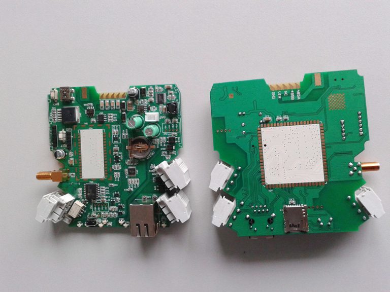
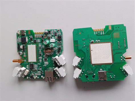
Effective PCB assembly for compact slingshot-style devices demands precision in balancing miniaturization with structural resilience. Engineers prioritize shockproof layouts by clustering critical components near the board’s geometric center, reducing leverage points that amplify mechanical stress. This approach is particularly vital in PCBA designs where high-density interconnects must coexist with reinforced mounting points for external hardware.
Strategic use of flexible substrates combined with rigid sections enhances durability while maintaining the slender profiles required for rugged applications. Vibration-resistant soldering techniques, such as low-voiding solder pastes and conformal coatings, mitigate fatigue failures at joints exposed to repetitive impacts. Component stacking optimization further minimizes vertical space usage without compromising thermal management—key for electronics operating in fluctuating temperatures.
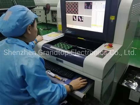
To ensure reliability, designers integrate redundant traces and staggered via placements, which distribute stress more evenly across the board. Advanced PCB assembly workflows now incorporate automated optical inspection (AOI) systems to detect micro-fractures or misalignments early in production. These tactics collectively address the unique challenges of embedding robust circuitry into compact, high-stress environments while adhering to stringent ruggedization standards.
Shockproof Layouts for Rugged Electronics
Designing PCB assembly layouts for rugged devices demands strategic planning to mitigate mechanical stress and environmental impacts. Central to shockproof design is the placement of high-mass components near the board’s center, reducing leverage effects during sudden impacts. Engineers prioritize PCBA configurations with reinforced mounting points for connectors and sensors, using flexible substrates like polyimide to absorb vibrational energy. Critical traces are routed diagonally or in curved patterns to avoid stress concentration zones, while high-Tg laminates enhance thermal stability under rapid temperature fluctuations.
To address multidirectional forces, cross-bracing techniques in PCB assembly involve interleaving ground planes between signal layers, improving structural rigidity. Components susceptible to shear forces, such as ceramic capacitors, are positioned away from board edges and secured with underfill adhesives. Additionally, conformal coatings with silicone or urethane bases provide an extra barrier against moisture and particulate ingress. By integrating these shockproof strategies into PCBA workflows, manufacturers ensure reliable operation in applications ranging from industrial automation to military-grade equipment, laying the foundation for subsequent vibration-resistant soldering and stacking optimizations.

Vibration-Resistant Soldering Techniques
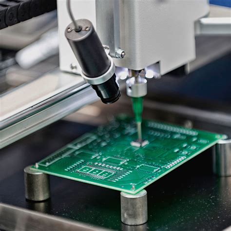
Achieving reliable connections in PCB assembly for rugged devices demands specialized soldering methods that withstand sustained mechanical stress. Unlike standard PCBA processes, vibration-resistant techniques prioritize joint integrity and material flexibility to mitigate micro-fractures caused by repetitive shocks. One critical approach involves using high-tin solder alloys (e.g., SAC305) with enhanced ductility, which absorb energy from vibrations without compromising electrical continuity.
For components exposed to extreme motion, underfill epoxy applications add structural support by filling gaps between chips and substrates, distributing stress evenly. Similarly, conformal coatings like silicone or polyurethane act as dampening layers, reducing resonance effects on solder joints. Advanced PCBA workflows integrate laser reflow soldering to create precise, void-free bonds, particularly for fine-pitch components where traditional methods risk incomplete adhesion.
Transitioning from design to execution, engineers must balance thermal management with mechanical resilience. For example, strain relief features such as curved traces or anchor points minimize tension on solder points during flexing. Pairing these strategies with rigorous vibration testing (e.g., MIL-STD-810G compliance) ensures PCB assemblies maintain functionality in environments ranging from industrial machinery to off-grid sensor networks. By prioritizing these methodologies, manufacturers elevate durability without sacrificing the compact form factors essential for modern rugged electronics.
Component Stacking Optimization Methods
Effective PCB assembly for rugged devices demands strategic component stacking to balance spatial efficiency with environmental resilience. In high-vibration applications, vertical integration of components through 3D packaging reduces footprint while maintaining structural integrity. Engineers must prioritize thermal management by alternating heat-generating ICs with passive elements, leveraging thermal vias and conductive adhesives to dissipate energy across layers.
Advanced PCBA techniques employ asymmetric stacking configurations, where critical components occupy central positions to minimize stress concentration during mechanical shocks. This approach requires precise alignment of ball grid arrays (BGAs) and surface-mount devices (SMDs) to prevent solder joint fractures. For extreme environments, hybrid stacks combining rigid and flexible substrates enable dynamic load distribution, with conformal coatings applied between layers to dampen resonant frequencies.
Transitioning between stacked modules, designers should implement graded stiffness zones—progressively increasing material rigidity from the PCB’s core to its periphery. This method enhances shock absorption without compromising signal integrity in multi-board systems. Automated optical inspection (AOI) becomes crucial here, verifying solder fillet geometries in tight interlayer spaces. By optimizing component density ratios and employing vibration-tolerant mounting patterns, manufacturers achieve durable electronics capable of withstanding prolonged exposure to harsh operational conditions.
Durable PCB Designs for Harsh Environments
Creating PCB assembly solutions for rugged devices demands meticulous attention to material selection and structural integrity. Engineers prioritize substrates with high thermal stability and moisture resistance, such as FR-4 variants with glass transition temperatures (Tg) exceeding 170°C or polyimide-based laminates. These materials mitigate warping and delamination risks under extreme temperature fluctuations common in industrial or outdoor settings.
To enhance durability, PCBA layouts incorporate redundant vias, thickened copper traces (2 oz/ft² or higher), and corner chamfering to reduce mechanical stress concentrations. Conformal coatings—like acrylic or silicone-based options—are applied post-assembly to shield components from dust, humidity, and chemical exposure. For high-vibration environments, stitched grounding and strategic placement of surface-mount devices (SMDs) minimize solder joint fatigue, while through-hole components with clinched leads add mechanical anchoring.
Designers also leverage edge-mounted connectors and encapsulated modules to protect sensitive interfaces from physical impacts. Thermal management is addressed through copper pours connected to heatsinks, ensuring efficient dissipation in compact form factors. By aligning PCB assembly techniques with MIL-STD-810 or IP67 standards, manufacturers achieve robust ruggedization without compromising the density required for modern slingshot-inspired device architectures. This integration of material science and layout optimization ensures reliable operation in environments where shock, vibration, and temperature extremes are unavoidable.
Rugged Device Integration Strategies
Integrating PCBA into rugged devices demands meticulous attention to mechanical resilience and environmental adaptability. Designers must prioritize shock-absorbent materials and PCB assembly techniques that withstand extreme vibrations, thermal cycling, and moisture ingress. For instance, employing conformal coatings enhances protection against dust and humidity, while strategic placement of high-stress components minimizes flex-induced failures.
A critical aspect involves balancing component stacking optimization with thermal management. Dense layouts risk overheating, so integrating thermally conductive substrates or heat-spreading vias becomes essential. Below is a comparison of design approaches for standard vs. rugged PCBA:
| Design Factor | Standard PCBA | Rugged PCBA |
|---|---|---|
| Component Spacing | 0.5–1.0 mm | 1.2–2.0 mm (vibration buffer) |
| Solder Type | Lead-free SAC305 | High-reliability alloys (e.g., SnAgCu+Bi) |
| Coating Thickness | 25–75 μm | 75–150 μm (enhanced sealing) |
Transitioning from shockproof layouts to integration, engineers should adopt modular designs for easier field repairs. For example, isolating sensitive circuits in shielded compartments reduces EMI interference while maintaining structural integrity. Additionally, leveraging vibration-resistant soldering methods—such as underfill adhesives or corner-bonded BGA packages—ensures lasting connections under repetitive stress. By aligning PCB assembly workflows with these strategies, manufacturers achieve seamless compatibility between compact form factors and rugged operational demands.
Advanced PCB Assembly for Durability
Modern PCB assembly processes for rugged devices demand precision engineering to withstand extreme mechanical stress. By integrating shock-absorbent underfill materials and PCBA-specific reinforcement protocols, manufacturers can significantly enhance structural integrity. Critical to this approach is the strategic placement of stress-sensitive components away from high-flex zones, combined with multi-axis solder joint inspections to identify micro-fractures before deployment.
Advanced conformal coatings, such as polyurethane or silicone-based formulations, create moisture-resistant barriers while maintaining thermal conductivity—a necessity for electronics operating in fluctuating temperatures. For PCB assembly in vibration-prone environments, stencil-designed solder paste patterns with higher viscosity alloys improve joint resilience, reducing fatigue failures by up to 40%.
Component anchoring techniques, including epoxy staking and corner-bonded ICs, further stabilize PCBA structures against repetitive impacts. Transitioning to rigid-flex PCB architectures allows seamless integration with shock-absorbing enclosures, merging durability with space efficiency. These methodologies align with MIL-STD-810G compliance benchmarks, ensuring reliable performance in industrial, automotive, and military applications where environmental extremes are unavoidable.
Harsh Environment Electronics Manufacturing
Designing PCB assembly solutions for harsh environments demands precision in balancing miniaturization with mechanical resilience. Manufacturers must account for extreme temperature fluctuations, moisture ingress, and sustained mechanical stress when selecting materials and processes. High-reliability PCBA designs often employ high-Tg substrates (e.g., polyimide) to withstand thermal cycling, while conformal coatings or silicone underfills protect against humidity and chemical exposure.
To mitigate vibration-induced failures, strain relief features—such as corner anchors and flexible interconnects—are integrated into PCB assembly layouts. Component placement follows zonal isolation principles, segregating sensitive ICs from high-vibration areas. Advanced soldering techniques, including laser reflow and low-void solder pastes, ensure joints remain intact under repetitive shocks.
Environmental testing protocols like thermal shock cycling and random vibration profiling validate PCBA durability before deployment. These protocols align with IPC-6012 Class 3 standards, which mandate stricter tolerances for military and industrial applications. By combining robust material science with adaptive manufacturing workflows, engineers achieve field-ready electronics capable of enduring decades in demanding operational settings.
Conclusion
Effective integration of PCB assembly techniques into rugged device manufacturing demands a holistic approach that balances miniaturization with durability. By prioritizing shockproof layouts and vibration-resistant soldering methods, engineers can mitigate mechanical stress in harsh operational environments. Strategic PCBA workflows, including optimized component stacking and material selection, further enhance structural integrity while maintaining compact form factors. These practices not only extend product lifespans but also reduce failure rates in applications exposed to extreme temperatures, moisture, or repetitive impacts. As industries increasingly rely on electronics in demanding settings, adopting these advanced PCB assembly strategies ensures devices meet rigorous performance standards without compromising on reliability or spatial efficiency.
FAQs
How does component stacking affect durability in rugged PCBAs?
PCB assembly processes that employ vertical component stacking enhance spatial efficiency while maintaining structural integrity. By using 3D packaging techniques, engineers can reduce board footprint without compromising shock absorption capabilities, critical for devices in harsh environments.
What soldering methods improve vibration resistance?
Low-void soldering combined with underfill encapsulation ensures joints withstand repetitive stress. For PCBA in rugged applications, techniques like conformal coating and selective stiffener placement further mitigate micro-fracture risks during prolonged vibration exposure.
Are there layout standards for shockproof designs?
Yes. Implementing decoupling capacitors near high-power components and avoiding right-angle traces are key. PCB assembly guidelines for rugged devices often prioritize symmetrical component placement and redundant grounding to distribute mechanical stress evenly.
How do material choices impact harsh-environment performance?
High-Tg laminates and ceramic-filled substrates excel in thermal cycling scenarios. For PCBA longevity, pairing these with environmentally sealed connectors and corrosion-resistant finishes ensures reliability in extreme humidity or temperature fluctuations.
Can compact designs maintain MIL-STD compliance?
Absolutely. Advanced PCB assembly strategies, such as embedded component technology and laser-drilled microvias, enable miniaturization while meeting MIL-STD-810G shock/vibration thresholds. Rigorous simulation testing validates compliance before production.
Ready to Optimize Your Rugged PCB Assembly?
For tailored solutions in durable PCBA design and manufacturing, please click here to connect with our engineering team. Explore cutting-edge techniques for harsh-environment electronics tailored to your project’s demands.