Comprehensive Guide to PCB Routing: Ensuring Signal Integrity and Optimal Performance
Introduction
Printed Circuit Boards (PCBs) are the backbone of modern electronics, serving as the foundation for the interconnection and support of various electronic components. One of the most critical aspects of PCB design is routing, which involves creating the conductive pathways (traces) that connect components and allow electrical signals to flow. Proper PCB routing is essential for ensuring signal integrity, minimizing electromagnetic interference (EMI), and achieving optimal performance. This article provides an in-depth exploration of PCB routing, covering its principles, techniques, design considerations, and the latest trends in routing technology.
1. Understanding PCB Routing
1.1. What is PCB Routing?
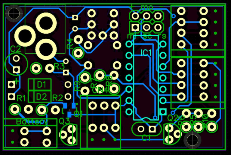
PCB routing is the process of designing the conductive traces that connect the various components on a PCB. These traces carry electrical signals, power, and ground between components, enabling the circuit to function as intended. Routing involves determining the path, width, and layer of each trace, as well as ensuring that the design meets electrical, thermal, and mechanical requirements.
1.2. Types of Routing
There are several types of routing, each suited for different aspects of PCB design:
- Signal Routing: This involves routing the traces that carry electrical signals between components. Signal routing must consider factors such as signal integrity, impedance matching, and crosstalk.
- Power Routing: This involves routing the traces that distribute power and ground throughout the PCB. Power routing must consider factors such as current capacity, voltage drop, and thermal management.
- High-Speed Routing: This involves routing traces that carry high-speed signals, such as those in digital communication and RF circuits. High-speed routing must consider factors such as signal reflections, EMI, and timing constraints.
2. Principles of PCB Routing
2.1. Signal Integrity
Signal integrity is a critical consideration in PCB routing, especially for high-speed and high-frequency circuits.
- Impedance Matching: Proper impedance matching is essential to prevent signal reflections and degradation. This involves designing traces with controlled impedance, which depends on the trace width, thickness, and the dielectric properties of the PCB material.
- Crosstalk: Crosstalk occurs when signals from one trace interfere with adjacent traces. Proper spacing, shielding, and routing techniques can minimize crosstalk.
- Signal Reflections: Signal reflections can occur due to impedance mismatches at junctions, vias, and connectors. Proper termination and routing techniques can reduce reflections and improve signal integrity.
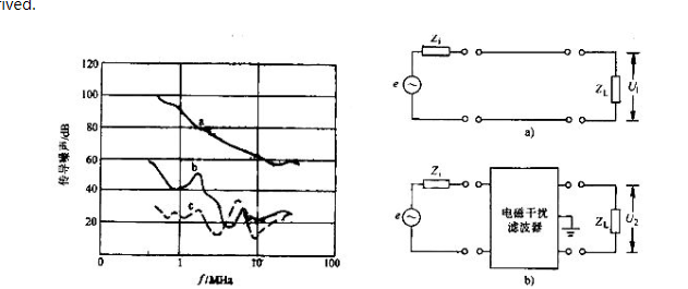
2.2. Electromagnetic Compatibility (EMC)
EMC is the ability of the PCB to function correctly in its electromagnetic environment without causing or suffering from interference.
- EMI Reduction: Proper routing techniques, such as minimizing loop areas, using ground planes, and routing differential pairs, can reduce EMI.
- Shielding: Shielding techniques, such as using ground planes and shielding cans, can protect sensitive circuits from external EMI.
- Filtering: Adding filters, such as ferrite beads and capacitors, can suppress noise and improve EMC.
2.3. Thermal Management
Thermal management is essential for ensuring the reliability and performance of the PCB.
- Heat Dissipation: Proper routing can help dissipate heat by providing low-resistance paths for heat to flow away from hot components.
- Thermal Vias: Thermal vias can be used to transfer heat from the surface layers to the inner layers or the opposite side of the PCB.
- Trace Width: Wider traces can carry more current and dissipate heat more effectively, but they also take up more space.
3. PCB Routing Techniques
3.1. Manual Routing
Manual routing involves manually placing and routing traces on the PCB layout. This technique offers maximum control and flexibility but can be time-consuming and prone to errors.
- Advantages: Full control over trace placement, ability to optimize for specific requirements.
- Disadvantages: Time-consuming, prone to human error, challenging for complex designs.
3.2. Auto-Routing
Auto-routing involves using software algorithms to automatically route traces on the PCB layout. This technique is faster and more consistent but may not always produce optimal results.
- Advantages: Fast, consistent, suitable for complex designs.
- Disadvantages: May require manual adjustments, limited by the quality of the routing algorithms.
3.3. Interactive Routing
Interactive routing combines manual and auto-routing techniques, allowing the designer to guide the auto-router while maintaining control over critical traces.
- Advantages: Balances control and speed, allows for optimization of critical traces.
- Disadvantages: Requires experience and skill, may still require manual adjustments.
4. Design Considerations for PCB Routing
4.1. Layer Stackup
The layer stackup of the PCB affects routing by determining the number of layers available for routing and the placement of power and ground planes.
- Signal Layers: The number of signal layers determines the routing density and complexity. More layers allow for more complex routing but increase cost.
- Power and Ground Planes: Power and ground planes provide low-impedance paths for power distribution and reduce EMI. Proper placement of these planes is essential for effective routing.
4.2. Trace Width and Spacing
The width and spacing of traces affect their electrical and thermal performance.
- Trace Width: Wider traces can carry more current and dissipate heat more effectively but take up more space. Narrower traces allow for higher routing density but have higher resistance and lower current capacity.
- Trace Spacing: Proper spacing between traces reduces crosstalk and EMI. The required spacing depends on the signal speed, voltage, and PCB material.
4.3. Via Placement
Vias are used to connect traces on different layers. Proper via placement is essential for minimizing signal integrity issues and ensuring efficient routing.
- Via Size: The size of the via affects its electrical and thermal performance. Smaller vias allow for higher routing density but have higher resistance and lower current capacity.
- Via Placement: Vias should be placed close to the components they connect to minimize trace length and reduce inductance. However, they should not be placed too close to avoid mechanical stress and soldering issues.
4.4. Differential Pair Routing
Differential pairs are used in high-speed and high-frequency circuits to improve signal integrity and reduce EMI.
- Length Matching: The lengths of the traces in a differential pair should be matched to minimize skew and maintain signal integrity.
- Spacing: The spacing between the traces in a differential pair should be consistent to maintain impedance matching and reduce crosstalk.
- Routing: Differential pairs should be routed together, avoiding sharp bends and crossing other traces.
5. Advanced Routing Techniques
5.1. High-Speed Routing
High-speed routing involves designing traces that carry high-speed signals, such as those in digital communication and RF circuits.
- Controlled Impedance: High-speed traces must have controlled impedance to prevent signal reflections and degradation. This involves designing traces with specific widths and spacing based on the PCB material and layer stackup.
- Length Matching: High-speed traces should be length-matched to minimize skew and maintain signal integrity.
- Termination: Proper termination, such as series or parallel termination, can reduce signal reflections and improve signal integrity.
5.2. Power Integrity
Power integrity involves ensuring that the power distribution network (PDN) delivers stable and clean power to all components.
- Decoupling Capacitors: Decoupling capacitors should be placed close to the power pins of components to reduce noise and stabilize the power supply.
- Power Planes: Power planes provide low-impedance paths for power distribution and reduce voltage drop. Proper placement and routing of power planes are essential for power integrity.
- Via Placement: Vias should be used to connect power and ground planes to the components, ensuring low-resistance paths for current flow.
5.3. RF and Microwave Routing
RF and microwave routing involves designing traces that carry high-frequency signals, such as those in wireless communication and radar systems.
- Impedance Matching: RF traces must have controlled impedance to prevent signal reflections and degradation. This involves designing traces with specific widths and spacing based on the PCB material and layer stackup.
- Shielding: RF traces should be shielded to reduce EMI and prevent interference with other circuits. This can be achieved using ground planes, shielding cans, and coaxial cables.
- Length Matching: RF traces should be length-matched to minimize skew and maintain signal integrity.
6. Latest Trends in PCB Routing
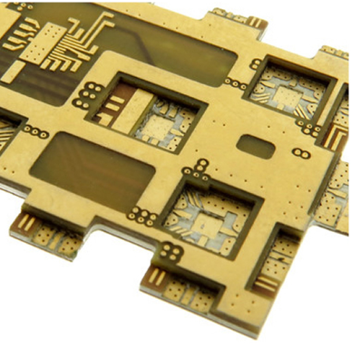
6.1. High-Density Interconnect (HDI) Routing
HDI routing involves designing PCBs with higher routing density, allowing for more complex and compact designs.
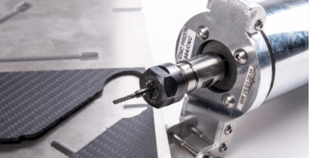
- Microvias: Microvias are small vias used in HDI PCBs to increase routing density and reduce board size.
- Laser Drilling: Laser drilling is used to create precise and small-diameter vias in HDI PCBs.
- Stacked and Staggered Vias: Stacked and staggered vias are used in HDI PCBs to connect multiple layers and increase routing density.
6.2. 3D Packaging and Integration
The trend towards 3D packaging and integration is driving the development of advanced routing techniques.
- Through-Silicon Vias (TSVs): TSVs are used in 3D ICs to connect multiple layers of silicon, enabling higher density and performance.
- Interposer Routing: Interposers use advanced routing techniques to connect different chips and components in a 3D package, improving signal integrity and thermal management.
6.3. Additive Manufacturing
Additive manufacturing, or 3D printing, is emerging as a potential method for creating PCBs with complex routing structures.
- Flexibility: Additive manufacturing allows for the creation of complex routing structures and custom designs.
- Rapid Prototyping: 3D printing enables rapid prototyping and testing of routing designs, reducing development time.
7. Conclusion
PCB routing is a critical aspect of ensuring the performance, reliability, and manufacturability of electronic devices. Proper routing involves careful consideration of signal integrity, EMC, thermal management, and design constraints, as well as adherence to routing guidelines and standards. Advanced routing techniques, such as high-speed routing, power integrity, and RF routing, are driving innovation in PCB design, enabling higher density and performance. As the electronics industry continues to evolve, PCB routing will play an increasingly important role in meeting the demands of high-speed, high-frequency, and 3D integrated circuits. By staying abreast of the latest trends and technologies in PCB routing, engineers and designers can create PCBs that deliver superior performance and reliability.