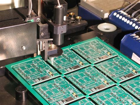
Conductive pattern wiring design
Wiring is to lay out printed conductors according to the electrical schematic or logic diagram and network table as well as the required wire width and spacing. The width and spacing of the wires cannot exceed the limit of the manufacturability requirements of the printed board. And the impact of manufacturing tolerances on the width and spacing of printed conductors should be considered. Whether the wiring is reasonable or not will affect the electrical performance, electromagnetic compatibility, warpage and manufacturability of the printed board. If you use CAD wiring. After importing the network table and component layout according to the program in Figure 8-3, you can formulate detailed wiring rules according to the following requirements and then carry out wiring.
1. Setting and allocation of wiring layers
On the premise of meeting the use requirements, considering the reliability and manufacturability of the product, the order of selecting wiring layers is single-layer, double-layer and multi-layer wiring. For high-frequency and digital circuits, it is best to use double-sided or multi-layer wiring, and set up the ground layer and power layer separately.
With the widespread application of digital circuits, the transmission rate of circuit signals continues to increase, especially high-frequency signals and differential signals have strict requirements on the impedance of wires. Therefore, when wiring, not only the wiring rate and wiring density of the wires should be considered, but also the characteristic impedance of the wires should be considered. The impedance is not only related to the impedance of the wire itself and the dielectric material, but also has an important relationship with the distribution of the wiring layer.

Therefore, after determining the number of wiring layers, the allocation of each wiring layer is also very important. The printed wires on the printed circuit board are mainly divided into ground wires, power wires, signal wires, and signal wires. Signal lines and other auxiliary lines. For single-sided printed circuit boards, of course, all wires must be laid on the same side. For double-sided boards, in low-frequency circuits, as long as the ground line and the power line are close to each other, they can be distributed on one or both sides of the board.
Signal lines can also be distributed on both sides, but the wiring on both sides should be balanced. However, in high-frequency circuits, high-frequency signal lines should be laid in the form of microstrip lines, that is, the signal line is on one side and the ground line is on the other side in a mirror-image layout, which is conducive to reducing impedance and radiation.
Multilayer board wiring can be specially set up with ground layers and power layers, which is more conducive to the layout of high-frequency signal lines. Multilayer boards use an even number of wiring layers, and the center of the board thickness is used as the symmetry axis to make the copper foil distribution basically symmetrical, so as to reduce the possibility of warping of the finished board. The following are several recommended wire layer distribution schemes for multilayer boards.

(1) Wire distribution for four-layer boards.
(2) Wire allocation for six-layer boards.
The above two solutions are the best ones, which can ensure that the signal has sufficient return area. The ground layer is close to the power layer, and the board has a large body capacitance, which is conducive to power decoupling. The only drawback is that the six-layer board has three ground and power layers, and the signal line wiring layer is a little less. If the wiring density needs to be very high, the wiring layer should be increased. There is another wiring solution for the six-layer board, that is, one ground layer can be reduced, and the high-frequency signal line is close to the ground layer. If there is a differential impedance requirement, the ground layer should be increased so that each signal line layer can be close to the ground layer.
This solution has one more signal line layer than the previous solution, and the wires of the two adjacent signal layers in the middle should be crossed to prevent signal crosstalk. High-frequency signals can return through the adjacent ground and power layers.
(3) Wire layer allocation for eight-layer boards.
(4) Wire layer allocation for ten-layer boards
On the ground layer, try to reduce the number of ground layer splits due to insufficient ground layer. Splitting can easily cause signal lines to cross the split grooves during wiring, causing electromagnetic interference problems. Separating the above ground layers is beneficial to electromagnetic compatibility, but the disadvantage is that increasing the number of wiring layers will increase the cost. However, according to the current processing technology level, the cost difference between 6-10 layer boards is not very large. For high-reliability printed circuit boards, the best cost-effectiveness should be selected to determine the number of wiring layers.
2.Wiring order
(1) After determining the allocation of wiring layers, first consider the structure and position of the ground layer and the power layer.
(2) The order of wiring in the same wiring layer is: first lay the ground line, then the power line, and finally the signal line (first high frequency and then low frequency).
(3) The wiring order of signal lines is: analog small signal lines, signal lines that are particularly sensitive to crosstalk, system clock signal lines, signal lines with high transmission delay requirements, general signal lines, static potential lines, and auxiliary lines.

3 Wiring requirements
(1) The layout of loop wires in the circuit should be kept to a minimum, and loop wires should be avoided. This is because loop wires are prone to electromagnetic radiation, which is equivalent to a loop antenna. They can both emit magnetic fields and receive spatial magnetic fields, and have poor electromagnetic compatibility.
(2) The wire layout between the two connection plates should be as short as possible, especially the input wires of the amplifier circuit and the high-frequency signal wires should be laid out at a short distance. A ground wire shield should be laid next to the input wires of the analog circuit.
(3) The printed wires on both sides of the double-sided board and the adjacent signal wire layers of the multi-layer board should be laid perpendicular to each other, or cross obliquely or bend to reduce parasitic capacitance.
(4) Try to avoid long-distance parallel wiring. The length of the wire between the two pads should comply with the principle of 1/20λ of the corresponding wavelength to reduce coupling capacitance and insulation resistance between wires.
(5) High-speed, high-frequency signal lines and signal lines of different frequencies should be laid out as close to each other and in parallel as possible to avoid signal interference.
If necessary, add a ground wire between the two signal lines for isolation; for high-frequency signal lines, a ground wire should be laid on one or both sides for shielding
(6) The bends of the wire should be right angles or obtuse angles.
If the bend angle is less than 90′, the outer edge of the bend should be made into an arc to avoid sharp corners. Because the stress on the sharp corners of the wire is concentrated during the manufacturing process, the wire is prone to warping. When the printed board is powered on, the tip is prone to discharge, which reduces the voltage between the wires. In high-frequency circuits, RF radiation is easily generated to cause electromagnetic interference.
(7) The layout of the wires on the same layer should be evenly distributed, and the conductive area on each wire layer should be relatively balanced
. This is to prevent the uneven distribution of metal conductors and the different thermal expansion coefficients with the base resin from causing internal stress to cause the printed board to warp and damage the plated holes and welding points.
(8) When connecting the printed wire to the pad, attention should be paid to the thermal distribution of the pad pattern to ensure that reliable solder joints can be formed during welding.
For through-hole installation, refer to the connection method between the wire and the pad below 1-4 in Figure 8-12. For surface-mounted printed boards, refer to the forms 5 and 6 in Figure 8-12. For pads on SMT printed boards, the wires should be led out from the middle of the pads. When the pads are connected to a larger conductive area, the length of the connection between the pads and the wires should be not less than 0.64mm. Thin wires with a width of not less than 0.13mm are thermally isolated (see the lower figure of 6 in Figure 8-12) to prevent the solder on the pad from being lost due to the capillary tube phenomenon caused by surface tension when the solder is wetted, which affects the quality of the solder joint.
(9) Component holes on wider printed conductors must be provided with pads (see the left figures of 2 and 3 in Figure 8-12) to facilitate easy identification of the hole position during drilling and inspection. It also helps to form a symmetrical circular solder joint centered on the component lead during welding.
(10) The connection end of the surface mounted BGA device is long.
A scattered connection plate is used under the device body to lead the signal line from the next layer through the via under the device. Or an extremely fine wire and a free angle are used to find a channel to lead out from the ball grid array of the pin (see Figure 8-13).
(11) When the wiring density is low, the width and spacing of the wire should be appropriately widened. The wire spacing of the printed circuit board used under low pressure conditions must also be widened. Especially for the 3rd level high reliability PCB design, the width and spacing of the printed wire must not only meet the minimum width and spacing requirements, but also leave a certain safety factor as much as possible. For example, the minimum wire width and spacing of a general PCB can be less than 0.13mm, but the British military PCB stipulates that it is greater than or equal to 0.13mm (except for high-density interconnect printed boards).
(12) For high-frequency and high-speed circuits, double-sided and multi-layer printed circuit boards should be designed as much as possible. Signal lines are laid on one side of the double-sided board, and the other side can be designed as a ground plane. In multi-layer boards, signal lines that are susceptible to interference can be arranged between ground layers or power layers or in conductor layers adjacent to ground layers or power layers.
(13) Avoid laying thin and long printed conductors. Although they do not exceed the specified electrical length, they will also increase the RF radiation of high-frequency signals.
(14) For the signal lines of differential circuits, a separate return line should be set. The return line and the original signal input line should be laid as close and parallel as possible. The line spacing can be small, which is conducive to the cancellation of magnetic fields and reduces signal interference. However, the minimum spacing should be greater than the limit of manufacturability.
(15) The transmission wires of the clock circuit and high-frequency circuit are the main sources of interference and radiation.
They should be laid out separately, away from the transmission lines of analog circuits and other sensitive circuits. When the wiring space allows, it is best to lay them in the middle of a large ground area to isolate them. In a multi-layer board, they can be laid near the ground layer or between the ground layer and the power layer of the multi-layer board.
(16) The clock and high-frequency circuit wires should be routed on the same layer as much as possible to reduce vias. Tree stump-type shunts and branching routing are not allowed (see the two figures on the left of Figure 8-14). This is because shunts will cause attenuation and reflection of the clock signal, resulting in signal deformation and possibly phase changes. High-frequency signal lines can be connected to other lines through holes in a daisy chain (see Figure 8-14), but vias should be minimized on the same line.
(17) The width of the same high-frequency signal line should be uniform to avoid wide sections and narrow sections. This will cause discontinuity in the impedance of the wire, making it difficult to control the impedance during design and easily generating electromagnetic radiation.
(1 8) Components or printed wires with large potential differences during operation should be kept at a greater distance from each other to prevent mutual influence. Strong current signal lines and weak current signal lines should be kept away from each other.
(19) The conductors and pads near the edge of the board should be no less than 5mm away from the edge of the printed board.
If a ground wire (or surface) is required, it can be close to the edge of the board. The signal layer and power layer conductors of the inner layer of the multi-layer printed board must be away from the edge of the board to avoid short circuits between layers when processing the printed board shape and cutting the residual metal debris or burrs on the edge of the board.
If the printed board is to be inserted into the guide rail, the distance between the conductor and the edge of the board should be slightly greater than the depth of the guide rail groove to avoid scratching the conductor or short circuiting the conductor when the conductor contacts the guide rail.
(20) If metal characters are required, they should be designed together during wiring. And the minimum conductor spacing regulations should be followed.


