Controlled impedance flex pcb
Understanding Controlled Impedance in Flex PCBs: A Comprehensive Guide
Controlled impedance in flexible printed circuit boards (flex PCBs) is a critical aspect of modern electronics design, particularly as devices become more compact and their functionalities more complex. Understanding controlled impedance is essential for engineers and designers who aim to ensure signal integrity and optimal performance in high-frequency applications. As electronic devices continue to shrink in size while increasing in capability, the demand for reliable and efficient flex PCBs with controlled impedance has grown significantly.
To begin with, controlled impedance refers to the precise management of the electrical impedance of a transmission line within a circuit.
This is crucial in high-speed digital and RF circuits where signal integrity can be compromised by impedance mismatches, leading to reflections, signal loss, and potential data errors. In flex PCBs, which are known for their ability to bend and conform to various shapes, maintaining controlled impedance is particularly challenging due to the inherent variability in their physical structure. However, achieving controlled impedance is vital for ensuring that signals are transmitted with minimal distortion and loss.
The design of flex PCBs with controlled impedance involves several key considerations.
First, the materials used in the construction of the PCB play a significant role. The dielectric constant of the substrate material, for instance, directly affects the impedance. Therefore, selecting materials with consistent dielectric properties is essential. Additionally, the thickness of the dielectric layer and the width and spacing of the conductive traces must be carefully calculated to achieve the desired impedance. These parameters are interdependent, and any variation can lead to significant changes in impedance.
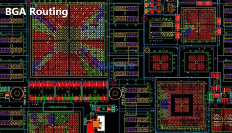
Moreover, the manufacturing process of flex PCBs must be meticulously controlled to maintain the designed impedance.
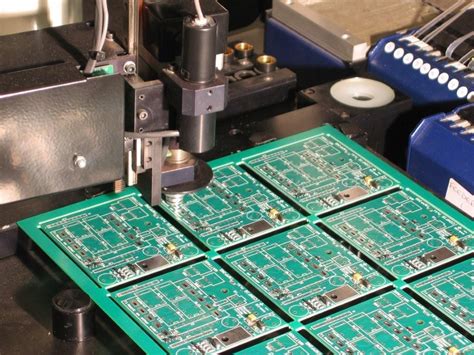
Variations in etching, lamination, and other fabrication steps can introduce discrepancies between the intended and actual impedance values. Therefore, manufacturers often employ advanced techniques such as laser direct imaging and precision etching to ensure that the physical dimensions of the traces and dielectric layers adhere closely to the design specifications.
Furthermore, testing and validation are integral components of the controlled impedance design process.
Engineers use tools such as time-domain reflectometry (TDR) and vector network analyzers to measure the impedance of the fabricated PCBs and verify that they meet the required specifications. These tests help identify any deviations from the desired impedance and allow for adjustments to be made in subsequent production runs.
In addition to the technical aspects, the application of controlled impedance flex PCBs spans a wide range of industries.
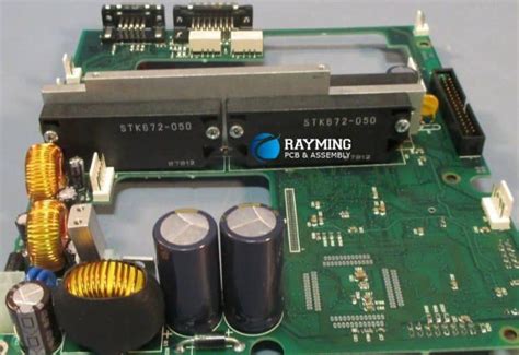
In telecommunications, for example, they are used in devices that require high-speed data transmission, such as smartphones and routers. In the automotive industry, flex PCBs with controlled impedance are employed in advanced driver-assistance systems (ADAS) and infotainment systems, where reliable signal transmission is crucial. The medical field also benefits from these PCBs in diagnostic equipment and wearable devices, where precision and reliability are paramount.
In conclusion, understanding and implementing controlled impedance in flex PCBs is a complex but essential task for ensuring the performance and reliability of modern electronic devices. By carefully considering material selection, design parameters, manufacturing processes, and rigorous testing, engineers can achieve the desired impedance characteristics. As technology continues to advance, the importance of controlled impedance in flex PCBs will only grow, making it a fundamental aspect of electronic design and manufacturing.
Design Tips for Achieving Controlled Impedance in Flexible Circuits
Achieving controlled impedance in flexible circuits is a critical aspect of modern electronic design, particularly as devices become more compact and complex. Controlled impedance ensures that signals are transmitted with minimal distortion, which is essential for maintaining the integrity of high-speed data communication. To achieve this, designers must consider several factors, including material selection, trace geometry, and layer configuration. By understanding these elements, engineers can create flexible circuits that meet the stringent requirements of today’s electronic applications.
One of the primary considerations in achieving controlled impedance is the selection of materials.
The dielectric constant of the substrate material plays a significant role in determining the impedance of a circuit. Flexible circuits often use polyimide or polyester substrates due to their excellent thermal and mechanical properties. However, these materials have different dielectric constants, which can affect impedance. Therefore, it is crucial to choose a substrate with a dielectric constant that aligns with the desired impedance specifications. Additionally, the thickness of the dielectric layer must be carefully controlled, as variations can lead to impedance mismatches.
Trace geometry is another critical factor in controlled impedance design.
The width and spacing of the traces, as well as their thickness, directly influence the impedance. Wider traces tend to have lower impedance, while narrower traces increase it. Similarly, the spacing between traces can affect crosstalk and signal integrity. To maintain controlled impedance, designers must calculate the optimal trace width and spacing based on the substrate’s dielectric properties and the desired impedance value. Advanced simulation tools can aid in this process, allowing designers to model different scenarios and select the best configuration.
Layer configuration also plays a vital role in achieving controlled impedance.
Flexible circuits can be single-layer, double-layer, or multi-layer, each offering different design possibilities and challenges. In multi-layer designs, the arrangement of signal and ground layers is crucial. A common approach is to use a ground plane adjacent to the signal layer, which helps to stabilize the impedance and reduce electromagnetic interference. The proximity of the ground plane to the signal traces can significantly impact the impedance, so precise control over layer thickness and spacing is necessary.
Moreover, the manufacturing process can introduce variations that affect controlled impedance.
Factors such as etching precision, material uniformity, and environmental conditions during production can lead to deviations from the intended design. To mitigate these issues, it is essential to work with experienced manufacturers who understand the intricacies of flexible circuit production. Implementing rigorous quality control measures and testing can also help ensure that the final product meets the desired impedance specifications.
In conclusion, achieving controlled impedance in flexible circuits requires a comprehensive understanding of material properties,
trace geometry, and layer configuration. By carefully considering these factors and utilizing advanced design tools, engineers can create flexible circuits that deliver reliable performance in high-speed applications. As technology continues to evolve, the demand for precise impedance control will only increase, making it imperative for designers to stay informed about the latest advancements and best practices in flexible circuit design. Through meticulous planning and collaboration with skilled manufacturers, achieving controlled impedance in flexible circuits is not only possible but essential for the success of modern electronic devices.
The Role of Material Selection in Controlled Impedance Flex PCB Design
In the realm of modern electronics, the demand for compact, efficient, and high-performance devices has led to the increased adoption of flexible printed circuit boards (PCBs). Among these, controlled impedance flex PCBs have emerged as a critical component in ensuring signal integrity, particularly in high-frequency applications. The role of material selection in the design of these PCBs cannot be overstated, as it directly influences the electrical performance, mechanical flexibility, and overall reliability of the circuit.
To begin with, controlled impedance is essential in applications where signal integrity is paramount, such as in telecommunications, medical devices, and aerospace systems.
The impedance of a circuit is determined by the physical dimensions of the conductors, the dielectric properties of the materials used, and the layout of the circuit. Therefore, selecting the appropriate materials is crucial to achieving the desired impedance levels. The dielectric constant and loss tangent of the substrate material are particularly important, as they affect the speed and attenuation of the signal traveling through the circuit.
Polyimide is a commonly used substrate material in flex PCBs due to its excellent thermal stability, mechanical flexibility, and favorable dielectric properties.
Its low dielectric constant and loss tangent make it an ideal choice for high-frequency applications, where minimizing signal loss is critical. However, other materials such as liquid crystal polymer (LCP) and polyethylene naphthalate (PEN) are also gaining popularity due to their unique properties. LCP, for instance, offers a lower moisture absorption rate and better dimensional stability, which can be advantageous in certain environments.
In addition to the substrate, the c#hoice of conductive materials plays a significant role in controlled impedance design.
Copper is the most widely used conductor due to its excellent electrical conductivity and ease of fabrication.
However, the thickness and width of the copper traces must be carefully controlled to maintain the desired impedance levels. In some cases, alternative materials such as silver or gold may be used to enhance performance, particularly in applications requiring high reliability and corrosion resistance.
Furthermore, the adhesive materials used in flex PCBs can impact the overall performance of the circuit.
Adhesives must provide strong bonding between the layers while maintaining flexibility and thermal stability. The choice of adhesive can also affect the dielectric properties of the circuit, thereby influencing impedance. As such, selecting an adhesive with a compatible dielectric constant is essential to maintaining controlled impedance.
The integration of these materials into a cohesive design requires careful consideration of the manufacturing process.
Techniques such as laser drilling, precision etching, and advanced lamination processes are often employed to achieve the precise dimensions and tolerances necessary for controlled impedance. Additionally, simulation tools and modeling software are invaluable in predicting the electrical performance of the circuit and optimizing the material selection.
In conclusion, the role of material selection in controlled impedance flex PCB design is multifaceted and critical to the success of the final product. By carefully choosing the substrate, conductive, and adhesive materials, designers can ensure that the circuit meets the stringent requirements of modern electronic applications. As technology continues to advance, the development of new materials and manufacturing techniques will undoubtedly further enhance the capabilities of controlled impedance flex PCBs, paving the way for even more sophisticated and reliable electronic devices.
Common Challenges and Solutions in Controlled Impedance Flex PCB Manufacturing
In the realm of modern electronics, controlled impedance flex PCBs have become a cornerstone for high-frequency applications, offering the flexibility and reliability required in advanced technological devices. However, the manufacturing of these sophisticated components is fraught with challenges that demand precise solutions to ensure optimal performance. Understanding these challenges and their corresponding solutions is crucial for manufacturers aiming to produce high-quality controlled impedance flex PCBs.
One of the primary challenges in manufacturing controlled impedance flex PCBs is maintaining consistent impedance across the board.
Impedance control is critical in high-speed circuits to prevent signal reflection and loss, which can degrade the performance of the device. Variations in impedance can arise from inconsistencies in the dielectric material, trace width, and spacing. To address this, manufacturers must employ rigorous material selection processes, ensuring that the dielectric constant of the substrate is uniform. Additionally, advanced fabrication techniques such as laser direct imaging can be utilized to achieve precise trace dimensions, thereby minimizing impedance variations.
Another significant challenge is the inherent flexibility of these PCBs, which can lead to mechanical stress and potential damage during the manufacturing process.
Flex PCBs are designed to bend and twist, but this flexibility can also make them susceptible to cracking or delamination. To mitigate this risk, manufacturers often incorporate protective layers and employ specialized handling techniques during production. Furthermore, the use of flexible adhesives and substrates that can withstand repeated bending without degrading is essential. By carefully selecting materials that offer both flexibility and durability, manufacturers can enhance the mechanical resilience of the final product.
Thermal management also poses a considerable challenge in the production of controlled impedance flex PCBs.
As electronic devices become more compact and powerful, the heat generated by components can lead to thermal stress, affecting the board’s performance and longevity. Effective thermal management solutions are therefore imperative. Manufacturers can integrate thermal vias and heat spreaders into the PCB design to facilitate heat dissipation. Additionally, selecting materials with high thermal conductivity can help manage heat more efficiently, ensuring that the PCB operates within safe temperature limits.
Moreover, the miniaturization trend in electronics adds another layer of complexity to the manufacturing process.
As devices shrink in size, the demand for smaller, more intricate flex PCBs increases. This miniaturization requires precise manufacturing techniques to ensure that the intricate patterns and fine traces are accurately produced. Advanced technologies such as laser drilling and high-resolution imaging systems are essential in achieving the necessary precision. These technologies allow for the creation of microvias and fine lines that are critical in modern electronic designs.
In conclusion, while the manufacturing of controlled impedance flex PCBs presents several challenges, these can be effectively addressed through careful material selection, advanced fabrication techniques, and innovative design solutions. By understanding and overcoming these challenges, manufacturers can produce high-quality flex PCBs that meet the demanding requirements of today’s electronic devices. As technology continues to evolve, the ability to adapt and innovate in the manufacturing process will remain a key factor in the successful production of controlled impedance flex PCBs.
Testing and Validation Techniques for Controlled Impedance in Flex PCBs
Controlled impedance in flexible printed circuit boards (flex PCBs) is a critical aspect of modern electronics design, particularly in applications requiring high-speed data transmission. Ensuring that these circuits perform optimally necessitates rigorous testing and validation techniques. These techniques are essential to confirm that the impedance values meet the specified requirements, thereby guaranteeing signal integrity and minimizing potential issues such as signal reflection and crosstalk.
To begin with, understanding the concept of controlled impedance is crucial.
Controlled impedance refers to the characteristic impedance of a transmission line, which is determined by the physical dimensions of the trace, the dielectric properties of the substrate, and the surrounding environment. In flex PCBs, achieving precise impedance control is more challenging than in rigid PCBs due to the inherent flexibility and variability in material properties. Therefore, meticulous design and manufacturing processes are required to maintain the desired impedance levels.
One of the primary testing techniques employed in validating controlled impedance in flex PCBs is Time Domain Reflectometry (TDR).
TDR is a powerful diagnostic tool that measures the impedance of a transmission line by sending a fast rise-time pulse down the line and observing the reflections. Any deviation from the expected impedance will result in a reflection, which can be analyzed to identify discontinuities or mismatches. TDR provides a detailed impedance profile along the length of the trace, allowing engineers to pinpoint specific areas that may require adjustment.
In addition to TDR, Vector Network Analysis (VNA) is another technique used to assess controlled impedance.
VNA measures the scattering parameters (S-parameters) of a transmission line, providing information about how signals are transmitted and reflected. By analyzing these parameters, engineers can determine the impedance characteristics and ensure they align with the design specifications. VNA is particularly useful for high-frequency applications, where precise impedance control is paramount.
Furthermore, simulation tools play a vital role in the validation process.
Before physical testing, engineers often use electromagnetic simulation software to model the flex PCB and predict its impedance characteristics. These simulations allow for the identification of potential issues and the optimization of the design before fabrication. By comparing simulation results with actual measurements, engineers can validate the accuracy of their models and make necessary adjustments to the design or manufacturing process.
Moreover, it is essential to consider the impact of environmental factors on impedance.
Flex PCBs are often subjected to varying temperatures, humidity levels, and mechanical stresses, all of which can affect impedance. Therefore, environmental testing is a crucial component of the validation process. By exposing the flex PCB to different conditions and measuring the impedance, engineers can ensure that the board will perform reliably in its intended application.
In conclusion, testing and validation techniques for controlled impedance in flex PCBs are indispensable for ensuring the performance and reliability of electronic devices.
Through the use of TDR, VNA, simulation tools, and environmental testing, engineers can accurately assess and validate the impedance characteristics of flex PCBs. These techniques not only help in identifying and rectifying potential issues but also contribute to the advancement of high-speed electronic applications, where controlled impedance is a fundamental requirement. As technology continues to evolve, the importance of precise impedance control in flex PCBs will only grow, underscoring the need for robust testing and validation methodologies.


