Creation pcb assembly
Understanding The Basics Of PCB Assembly: A Beginner’s Guide
Printed Circuit Board (PCB) assembly is a fundamental process in the electronics manufacturing industry, serving as the backbone for most electronic devices. Understanding the basics of PCB assembly is crucial for anyone interested in electronics, whether as a hobbyist or a professional.
This guide aims to provide a comprehensive overview of the essential components and processes involved in PCB assembly, offering a solid foundation for beginners.
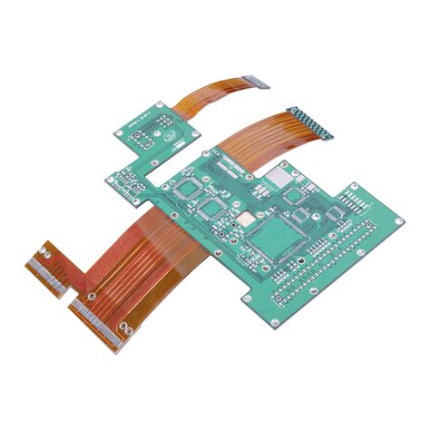
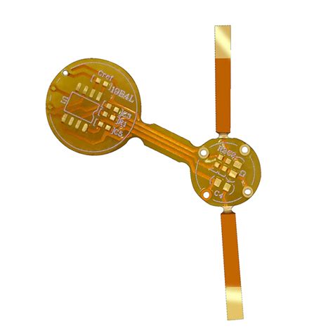
To begin with, a PCB is a flat board that physically supports and electrically connects electronic components using conductive pathways, tracks, or signal traces etched from copper sheets laminated onto a non-conductive substrate.
The assembly process involves several critical steps, starting with the design phase. During this phase, engineers use specialized software to create a schematic diagram, which serves as a blueprint for the PCB layout. This design is then translated into a physical board through a process called fabrication, where the board is manufactured according to the specified design.
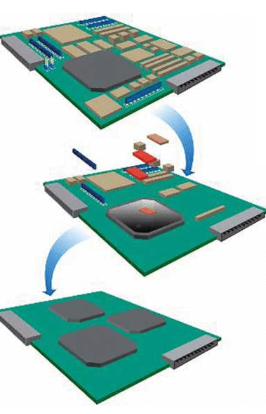
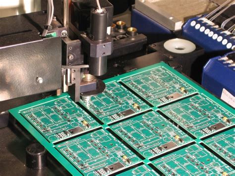
Once the PCB is fabricated, the next step is component placement.
This involves placing various electronic components, such as resistors, capacitors, and integrated circuits, onto the board. The placement can be done manually or through automated machines, depending on the complexity and scale of the production. Automated machines, known as pick-and-place machines, are commonly used in large-scale manufacturing due to their precision and efficiency.
Following component placement, the next crucial step is soldering.
Soldering is the process of joining the components to the PCB by melting solder around the connection points. This creates a strong electrical and mechanical bond. There are different soldering techniques, including wave soldering, reflow soldering, and hand soldering. Reflow soldering is widely used for surface-mount technology (SMT) components, where solder paste is applied to the board, and the entire assembly is heated in a reflow oven to melt the solder and secure the components.
After soldering, the assembled PCB undergoes inspection and testing to ensure functionality and reliability.
Inspection can be performed visually or using automated optical inspection (AOI) systems that detect defects such as misaligned components or soldering issues. Testing involves checking the electrical performance of the board to verify that it meets the design specifications. Functional testing may include powering the board and running specific tests to ensure all components operate correctly.
In addition to these steps, it is essential to consider the quality control measures throughout the PCB assembly process.
Quality control ensures that the final product is free from defects and meets industry standards. This involves adhering to guidelines such as the IPC standards, which provide criteria for the design, assembly, and testing of PCBs.
In conclusion, understanding the basics of PCB assembly involves familiarizing oneself with the design, fabrication, component placement, soldering, inspection, and testing processes. Each step is integral to producing a functional and reliable electronic device. As technology continues to advance, the complexity and capabilities of PCBs are expected to grow, making it even more important for beginners to grasp these foundational concepts. By doing so, they can better appreciate the intricacies of electronics manufacturing and contribute to the development of innovative electronic solutions.
The Role Of Surface Mount Technology In Modern PCB Assembly
Surface Mount Technology (SMT) has revolutionized the field of printed circuit board (PCB) assembly, playing a pivotal role in the advancement of modern electronics. As the demand for smaller, more efficient, and highly reliable electronic devices continues to grow, SMT has emerged as a critical component in meeting these requirements. This technology involves mounting electronic components directly onto the surface of PCBs, as opposed to the traditional method of inserting components through holes. The transition from through-hole technology to SMT has brought about significant improvements in the manufacturing process, leading to enhanced performance and miniaturization of electronic devices.
One of the primary advantages of SMT is its ability to accommodate a higher density of components on a PCB.
By eliminating the need for drilled holes, SMT allows for more components to be placed on both sides of the board, thereby maximizing the use of available space. This capability is particularly beneficial in the production of compact devices such as smartphones, tablets, and wearable technology, where space is at a premium. Furthermore, the reduced size of SMT components contributes to the overall miniaturization of electronic products, enabling manufacturers to design sleeker and more portable devices.
In addition to space efficiency, SMT offers significant improvements in the speed and cost-effectiveness of PCB assembly.
The automation of the SMT process allows for rapid placement of components, significantly reducing assembly time compared to manual through-hole insertion. This automation not only accelerates production but also enhances precision and consistency, minimizing the risk of human error. Consequently, manufacturers can achieve higher yields and lower production costs, making SMT an economically attractive option for large-scale production.
Moreover, SMT contributes to improved electrical performance and reliability of electronic devices.
The shorter lead lengths of SMT components result in lower parasitic inductance and capacitance, which enhances signal integrity and reduces electromagnetic interference. This is particularly important in high-frequency applications where signal quality is paramount. Additionally, the robust mechanical connection between SMT components and the PCB surface enhances the durability of the assembly, making it more resistant to mechanical stress and vibration. This reliability is crucial in applications where electronic devices are subjected to harsh environments or rigorous usage.
Despite its numerous advantages, SMT is not without its challenges.
The miniaturization of components necessitates precise placement and soldering techniques, requiring advanced equipment and skilled personnel. Furthermore, the inspection and testing of SMT assemblies can be more complex due to the high density of components and the potential for hidden solder joints.
However, advancements in inspection technologies, such as automated optical inspection (AOI) and X-ray inspection, have mitigated these challenges, ensuring the quality and reliability of SMT assemblies.
In conclusion, Surface Mount Technology has become an indispensable part of modern PCB assembly, driving innovation and efficiency in the electronics industry.
Its ability to support high-density component placement, coupled with its cost-effectiveness and enhanced performance, makes it a preferred choice for manufacturers aiming to produce cutting-edge electronic devices. As technology continues to evolve, SMT will undoubtedly play a crucial role in shaping the future of electronics, enabling the development of even more sophisticated and compact devices.
Key Challenges And Solutions In PCB Assembly Manufacturing
In the realm of electronics manufacturing, Printed Circuit Board (PCB) assembly stands as a critical process that bridges the gap between design and functional electronic devices. However, this intricate process is fraught with challenges that can impact both the efficiency and quality of the final product. Understanding these challenges and implementing effective solutions is essential for manufacturers striving to maintain competitiveness and meet the ever-evolving demands of the industry.
One of the primary challenges in PCB assembly is the increasing complexity of designs.
As electronic devices become more sophisticated, the PCBs that power them must accommodate a higher density of components and more intricate circuitry. This complexity can lead to difficulties in ensuring precise component placement and soldering, which are crucial for the functionality and reliability of the board.
To address this, manufacturers are turning to advanced automated assembly technologies, such as surface mount technology (SMT) and automated optical inspection (AOI) systems. These technologies enhance precision and reduce human error, thereby improving the overall quality of the assembly process.
Another significant challenge is the miniaturization of components.
As consumer demand pushes for smaller and more portable devices, components are becoming increasingly tiny, making them difficult to handle and place accurately on the PCB.
This miniaturization necessitates the use of specialized equipment and techniques, such as fine-pitch placement machines and micro-soldering tools, to ensure that even the smallest components are correctly positioned and securely attached.
Additionally, ongoing training and skill development for assembly technicians are vital to keep pace with these technological advancements and maintain high standards of workmanship.
Moreover, the rapid pace of technological change presents a constant challenge for PCB assembly manufacturers.
The industry is characterized by short product life cycles and frequent design updates, which require manufacturers to be agile and adaptable. To manage this, many companies are investing in flexible manufacturing systems that can quickly switch between different product lines and accommodate design changes with minimal downtime. This flexibility not only helps in meeting tight deadlines but also reduces the risk of obsolescence and waste.
Quality control is another critical area where challenges arise.
Ensuring that each PCB meets stringent quality standards is essential to prevent defects that could lead to device failures. Implementing robust quality assurance protocols, such as in-circuit testing (ICT) and functional testing, is crucial for identifying and rectifying issues early in the assembly process. Furthermore, adopting a culture of continuous improvement, where feedback from testing is used to refine processes and prevent future defects, can significantly enhance product reliability.
Environmental and regulatory compliance also pose challenges in PCB assembly manufacturing.
With increasing awareness of environmental issues, manufacturers must adhere to regulations such as the Restriction of Hazardous Substances (RoHS) directive, which limits the use of certain hazardous materials in electronic products. This requires careful selection of materials and processes that comply with these standards without compromising on performance or cost. Implementing sustainable practices, such as recycling and waste reduction, not only helps in meeting regulatory requirements but also enhances the company’s reputation and appeal to environmentally conscious consumers.
In conclusion, while PCB assembly manufacturing is fraught with challenges, there are numerous solutions available to address these issues effectively. By leveraging advanced technologies, fostering a skilled workforce, maintaining flexibility, ensuring rigorous quality control, and adhering to environmental regulations, manufacturers can overcome these challenges and continue to deliver high-quality, reliable electronic products. As the industry continues to evolve, staying ahead of these challenges will be key to sustaining success in the competitive landscape of electronics manufacturing.
Innovations In PCB Assembly: Trends Shaping The Future
The field of printed circuit board (PCB) assembly is undergoing a transformative phase, driven by rapid technological advancements and evolving industry demands.
As the backbone of modern electronic devices, PCBs are integral to the functionality and efficiency of a wide array of products, from consumer electronics to sophisticated industrial machinery. Consequently, innovations in PCB assembly are pivotal in shaping the future of electronics manufacturing, offering enhanced performance, reduced costs, and increased reliability.
One of the most significant trends in PCB assembly is the miniaturization of components.
As electronic devices become more compact and multifunctional, the demand for smaller, yet more powerful, PCBs has surged. This trend is facilitated by advancements in surface mount technology (SMT), which allows for the placement of smaller components on both sides of a PCB, thereby maximizing space utilization. Moreover, the development of microelectromechanical systems (MEMS) and advanced packaging techniques further supports this miniaturization, enabling the integration of more components into a single chip.
In addition to miniaturization, the push towards higher performance and efficiency is driving innovations in materials used for PCB assembly.
Traditional materials like FR-4 are being supplemented or replaced by advanced substrates such as polyimide and ceramic-based materials, which offer superior thermal management and electrical performance. These materials are particularly crucial in high-frequency applications and environments where thermal stability is paramount. Furthermore, the adoption of lead-free soldering techniques, in compliance with environmental regulations, is becoming more widespread, promoting sustainability without compromising on performance.
Another noteworthy trend is the increasing automation of PCB assembly processes.
Automation not only enhances precision and repeatability but also significantly reduces production time and labor costs. The integration of robotics and artificial intelligence (AI) in assembly lines is revolutionizing the industry, allowing for real-time monitoring and quality control. Machine learning algorithms are being employed to predict potential defects and optimize assembly processes, thereby minimizing waste and improving yield rates. This shift towards smart manufacturing is indicative of a broader trend towards Industry 4.0, where interconnected systems and data analytics play a central role in production.
Moreover, the rise of the Internet of Things (IoT) is influencing PCB assembly by necessitating the development of PCBs that can support wireless communication and connectivity.
This has led to innovations in antenna design and the incorporation of wireless modules directly onto PCBs. As IoT devices proliferate, the demand for PCBs that can seamlessly integrate with various communication protocols is expected to grow, further driving innovation in this area.
Finally, the trend towards customization and rapid prototyping is reshaping PCB assembly.
With the advent of 3D printing and other additive manufacturing techniques, it is now possible to produce custom PCBs quickly and cost-effectively. This capability is particularly beneficial for startups and small businesses, which can now iterate designs rapidly and bring products to market faster. Additionally, the use of digital twins and simulation software allows for virtual testing and optimization of PCB designs before physical production, reducing the risk of errors and enhancing design efficiency.
In conclusion, the future of PCB assembly is being shaped by a confluence of technological advancements and market demands. Miniaturization, material innovation, automation, IoT integration, and customization are key trends driving this evolution. As these innovations continue to unfold, they promise to enhance the capabilities and applications of PCBs, solidifying their role as a cornerstone of modern electronics.