Custom pcb board design
Understanding The Basics Of Custom PCB Design
Custom PCB board design is a critical aspect of modern electronics, serving as the backbone for a wide array of devices, from simple gadgets to complex machinery. Understanding the basics of custom PCB design is essential for engineers and hobbyists alike, as it lays the foundation for creating efficient, reliable, and innovative electronic products.
At its core, a printed circuit board (PCB) mechanically supports and electrically connects electronic components using conductive pathways, tracks, or signal traces etched from copper sheets laminated onto a non-conductive substrate. The customization of these boards allows for tailored solutions that meet specific requirements, enhancing the functionality and performance of the final product.
To begin with, the design process of a custom PCB involves several key steps, each requiring careful consideration and precision.
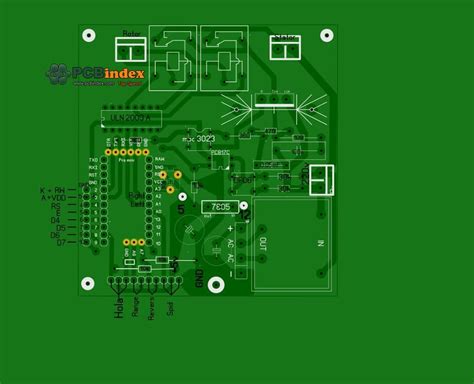
Initially, the designer must define the board’s requirements, including the size, shape, and the number of layers needed. This stage is crucial as it influences the overall complexity and cost of the project. Once the requirements are established, the next step is schematic capture, where the electronic circuit is represented in a diagrammatic form. This schematic serves as a blueprint for the PCB layout, detailing the components and their interconnections.
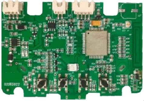
Following the schematic capture, the layout design phase commences.
During this phase, designers use specialized software tools to position components on the board and route the electrical connections between them. The layout must adhere to design rules and constraints, such as trace width, spacing, and layer stack-up, to ensure signal integrity and manufacturability. Moreover, designers must consider thermal management, as excessive heat can degrade performance or damage components. By strategically placing components and incorporating thermal vias or heat sinks, designers can mitigate thermal issues effectively.
Transitioning from design to production, the next step involves generating the necessary files for manufacturing.
These files, often in Gerber format, contain detailed information about each layer of the PCB, including copper traces, solder mask, and silkscreen. Additionally, a bill of materials (BOM) is prepared, listing all components required for assembly. It is imperative to verify these files through design rule checks (DRC) and electrical rule checks (ERC) to identify and rectify any potential errors before fabrication.
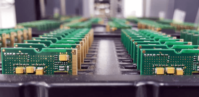
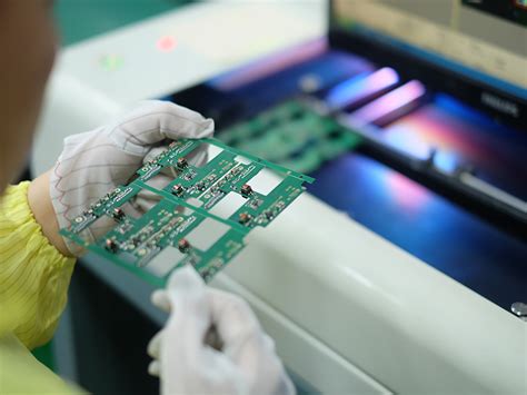
Once the design is finalized and verified, the manufacturing process begins.
This involves several stages, including etching, drilling, plating, and solder mask application, each contributing to the creation of the physical board. Quality control measures, such as automated optical inspection (AOI) and electrical testing, are employed to ensure the board meets the specified standards and functions as intended.
In conclusion, custom PCB board design is a multifaceted process that demands a thorough understanding of both theoretical principles and practical considerations.
By mastering the basics, designers can create bespoke solutions that not only meet the technical requirements but also push the boundaries of innovation. As technology continues to evolve, the role of custom PCB design becomes increasingly significant, underscoring its importance in the development of cutting-edge electronic devices. Through meticulous planning, precise execution, and continuous learning, designers can harness the full potential of custom PCB design to drive technological advancement.
Key Considerations For Designing High-Performance PCBs
Designing high-performance printed circuit boards (PCBs) is a complex task that requires careful consideration of various factors to ensure optimal functionality and reliability. As technology continues to advance, the demand for more efficient and compact electronic devices has increased, making the role of custom PCB design more critical than ever. To achieve high performance, designers must pay attention to several key considerations that can significantly impact the final product.
Firstly, the choice of materials is paramount in custom PCB design.
The substrate material, typically FR-4, must be selected based on the specific requirements of the application, such as thermal conductivity, dielectric constant, and mechanical strength. High-frequency applications may require materials with lower dielectric losses, while high-power applications might necessitate substrates with superior thermal management properties. By selecting the appropriate materials, designers can enhance the performance and longevity of the PCB.
In addition to material selection, the layout of the PCB plays a crucial role in its performance.
A well-thought-out layout minimizes electromagnetic interference (EMI) and crosstalk, which can degrade signal integrity. To achieve this, designers should carefully plan the placement of components and routing of traces. Utilizing techniques such as differential pair routing and controlled impedance can help maintain signal quality. Furthermore, ensuring adequate spacing between traces and components can prevent unwanted interactions and improve overall performance.
Another important consideration is the power distribution network (PDN) design.
A robust PDN ensures that all components receive stable and sufficient power, which is essential for high-performance operation. Designers should focus on minimizing voltage drops and noise in the power supply lines by using techniques such as power planes and decoupling capacitors. Additionally, attention should be given to the placement of vias and the use of multiple ground planes to reduce inductance and improve power delivery.
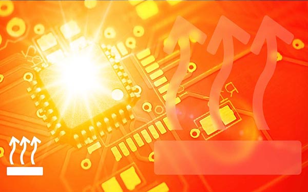
Thermal management is also a critical aspect of high-performance PCB design.
As electronic devices become more powerful, they generate more heat, which can adversely affect performance and reliability. Effective thermal management strategies, such as the use of thermal vias, heat sinks, and thermal pads, can help dissipate heat away from critical components. Moreover, selecting materials with high thermal conductivity and designing for optimal airflow can further enhance thermal performance.
Signal integrity is another key factor that must be addressed in custom PCB design.
High-speed signals are particularly susceptible to degradation due to factors such as impedance mismatches, reflections, and attenuation. To mitigate these issues, designers should employ techniques such as impedance matching, proper termination, and the use of high-quality connectors. Additionally, simulation tools can be invaluable in predicting and addressing potential signal integrity problems before the PCB is manufactured.
Finally, manufacturability and testing should not be overlooked in the design process.
Ensuring that the PCB can be easily manufactured and tested can save time and reduce costs. Designers should consider factors such as panelization, test point accessibility, and design for testability (DFT) to facilitate efficient production and quality assurance.
In conclusion, designing high-performance PCBs requires a comprehensive approach that considers material selection, layout, power distribution, thermal management, signal integrity, and manufacturability. By addressing these key considerations, designers can create custom PCBs that meet the demanding requirements of modern electronic devices, ensuring both performance and reliability. As technology continues to evolve, staying informed about the latest design techniques and tools will be essential for success in this ever-changing field.
Common Mistakes To Avoid In PCB Design
In the realm of electronics, custom PCB board design is a critical process that requires precision and attention to detail. However, even seasoned designers can fall prey to common mistakes that can compromise the functionality and reliability of the final product. Understanding these pitfalls is essential for anyone involved in PCB design, as it can save time, reduce costs, and enhance the overall quality of the board.
One of the most frequent errors in PCB design is inadequate planning.
Designers often rush into the layout phase without thoroughly considering the circuit’s requirements and constraints. This oversight can lead to inefficient use of space, increased complexity, and potential signal integrity issues. To avoid this, it is crucial to begin with a comprehensive schematic that clearly outlines the connections and components involved. By doing so, designers can ensure that the layout process is guided by a well-defined blueprint, minimizing the risk of errors.
Another common mistake is neglecting to adhere to design rules and guidelines.
Each PCB design is subject to specific constraints, such as trace width, spacing, and layer stack-up, which are dictated by the manufacturing process and the intended application. Ignoring these rules can result in boards that are difficult or impossible to manufacture, leading to costly redesigns and delays. Therefore, it is imperative to familiarize oneself with the design specifications and to utilize design rule checks (DRC) throughout the process to ensure compliance.
Furthermore, improper component placement can significantly impact the performance of a PCB.
Components should be strategically positioned to minimize trace lengths and reduce electromagnetic interference (EMI). Placing components too close together can lead to thermal issues, while excessive spacing can increase the board’s size and cost. To mitigate these risks, designers should prioritize the placement of critical components, such as power supplies and high-speed signals, and consider the thermal and electrical implications of their layout decisions.
In addition to component placement, trace routing is another area where mistakes frequently occur.
Poor routing can lead to signal integrity problems, such as crosstalk and impedance mismatches, which can degrade the performance of the circuit. To avoid these issues, designers should aim for direct and short trace paths, use appropriate trace widths, and implement proper grounding techniques. Additionally, employing differential pairs for high-speed signals and maintaining consistent trace impedance can further enhance signal integrity.
Moreover, overlooking the importance of power distribution can have detrimental effects on a PCB’s functionality.
Inadequate power distribution can result in voltage drops, noise, and overheating, which can compromise the performance and reliability of the board. To address this, designers should ensure that power and ground planes are properly sized and positioned, and that decoupling capacitors are strategically placed to stabilize voltage levels and filter out noise.
Finally, failing to conduct thorough testing and validation can lead to undetected errors that manifest in the final product.
Prototyping and simulation are essential steps in the design process, allowing designers to identify and rectify issues before mass production. By investing time in these validation processes, designers can ensure that the PCB meets all functional and performance requirements.
In conclusion, avoiding common mistakes in custom PCB board design requires careful planning, adherence to design rules, strategic component placement, effective trace routing, robust power distribution, and comprehensive testing. By being mindful of these factors, designers can create high-quality PCBs that meet the demands of modern electronic applications.

Innovations In Custom PCB Manufacturing Techniques
In recent years, the field of custom PCB (Printed Circuit Board) design has witnessed remarkable innovations, driven by the increasing demand for more efficient, compact, and versatile electronic devices. As technology continues to evolve, the manufacturing techniques for custom PCBs have undergone significant transformations, enabling designers to push the boundaries of what is possible in electronic design. These advancements not only enhance the functionality and performance of electronic devices but also contribute to the overall efficiency of the manufacturing process.
One of the most notable innovations in custom PCB manufacturing is the advent of advanced materials.
Traditionally, PCBs were made using materials like FR-4, a composite of woven fiberglass cloth with an epoxy resin binder. However, the introduction of new materials such as high-frequency laminates and flexible substrates has revolutionized the industry. These materials offer superior thermal management, reduced signal loss, and increased flexibility, making them ideal for applications in high-speed communication devices and wearable technology. Consequently, designers can now create PCBs that are not only more efficient but also more adaptable to various form factors.
In addition to material advancements, the integration of cutting-edge fabrication techniques has played a crucial role in the evolution of custom PCB design.
Techniques such as laser direct imaging (LDI) and additive manufacturing have significantly improved the precision and accuracy of PCB production. LDI, for instance, allows for the direct transfer of circuit patterns onto the PCB substrate using a laser, eliminating the need for traditional photomasks. This results in higher resolution and finer line widths, which are essential for the miniaturization of electronic components.
Similarly, additive manufacturing, or 3D printing, has opened new avenues for creating complex PCB structures with intricate geometries that were previously unattainable with conventional methods.
Moreover, the rise of automation and artificial intelligence in PCB manufacturing has streamlined the design and production process.
Automated design tools, powered by AI algorithms, can optimize circuit layouts, predict potential design flaws, and suggest improvements, thereby reducing the time and cost associated with PCB development. This level of automation not only enhances the efficiency of the manufacturing process but also ensures a higher degree of accuracy and reliability in the final product. As a result, manufacturers can meet the growing demand for custom PCBs with shorter lead times and greater consistency.
Furthermore, the implementation of environmentally friendly practices in PCB manufacturing has gained traction, reflecting a broader trend towards sustainability in the electronics industry.
Innovations such as waterless processing, lead-free soldering, and the use of biodegradable materials are becoming increasingly common. These practices not only reduce the environmental impact of PCB production but also align with the global push towards greener manufacturing processes. By adopting these sustainable techniques, manufacturers can minimize waste, conserve resources, and contribute to a more sustainable future.
In conclusion, the innovations in custom PCB manufacturing techniques have significantly transformed the landscape of electronic design. Through the development of advanced materials, the adoption of cutting-edge fabrication methods, the integration of automation and AI, and the implementation of sustainable practices, the industry has made great strides in enhancing the performance, efficiency, and environmental impact of custom PCBs. As technology continues to advance, it is likely that these innovations will further evolve, paving the way for even more sophisticated and sustainable electronic solutions.