Flex pcb through hole
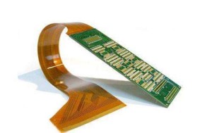
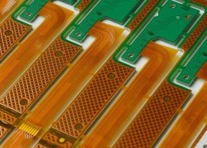
A flexible printed circuit board (flex PCB) with through-hole technology refers to a circuit board that has both surface mount components and through-hole components.
The through-hole components are mounted on the flexible substrate by inserting their leads through holes in the substrate and soldering them to the conductive traces on the opposite side of the board.
This type of flex PCB is commonly used in applications where a combination of surface mount and through-hole components are required,
such as in medical devices, aerospace, and automotive applications.
The use of through-hole technology provides additional mechanical stability and durability to the flex PCB,
making it more resistant to vibration and shock.

the role of flex pcb through hole
The role of flex PCB with through-hole technology is to provide a flexible circuit board solution that can accommodate both surface mount and through-hole components.
This type of flex PCB is used in applications where a combination of surface mount and through-hole components are required,
such as in medical devices, aerospace, and automotive applications.
The through-hole technology provides additional mechanical stability and durability to the flex PCB,
making it more resistant to vibration and shock. It also allows for better heat dissipation,
which is important in high-power applications.
The through-hole components can be larger and have higher power ratings than surface mount components,
making them suitable for applications that require higher current or voltage.
Flex PCB with through-hole technology also offers design flexibility,
allowing for the placement of components on both sides of the board.
This can help reduce the size of the PCB and increase the functionality of the device.
Additionally, the flexibility of the substrate allows for the PCB to be bent or folded, making it ideal for applications where space is limited.
Overall, the role of flex PCB with through-hole technology is to provide a reliable and flexible circuit board solution that can accommodate a wide range of components and applications.

flex pcb via in pad
Flex PCB via in pad refers to the process of placing a via (a small hole) directly in the pad of a flexible printed circuit board (PCB).
This technique is used to save space and reduce the number of layers required in a PCB design.
By placing the via in the pad, the connection between the top and bottom layers of the PCB can be made without the need for a separate via or trace.
This allows for more efficient use of space and can reduce the overall size of the PCB.
However, this technique can also pose challenges in terms of manufacturing and reliability,
as the via can affect the flexibility and durability of the PCB.

How does the flexible printed circuit board pass through the pad
During the manufacturing process of a flexible printed circuit board (PCB),
the via is drilled through the pad using a laser or mechanical drill.
The via is then plated with a conductive material, such as copper,
to create a connection between the top and bottom layers of the PCB.
In the case of a flex PCB via in pad, the via is drilled directly into the pad of the PCB,
which is typically a small circular or square area of copper that serves as a contact point for a component or trace.
The via is then plated with copper to create a conductive path that passes through the pad.
The use of a via in pad allows for a more compact and efficient PCB design,
as it eliminates the need for a separate via or trace to connect the top and bottom layers of the PCB.
However, this technique can also pose challenges during manufacturing and assembly,
as the via can affect the flexibility and durability of the PCB.
the role of Flexible printed circuit board via solder pads
The role of flexible printed circuit board (PCB) via solder pads is to provide a connection point between the PCB and the components that will be mounted on it.
The via solder pads are typically small circular or square areas of copper that are located on the surface of the PCB and are designed to receive solder.
When a component is mounted on the PCB, its leads or terminals are inserted through the via solder pads and then soldered in place.
This creates a secure and reliable electrical connection between the component and the PCB.
The use of via solder pads is particularly important in flexible PCBs, as they allow for a more compact and flexible design.
The via solder pads can be placed in close proximity to each other, allowing for a higher density of components to be mounted on the PCB.
Additionally, the use of via solder pads can help to reduce the overall size and weight of the PCB, making it ideal for applications where space is limited.
