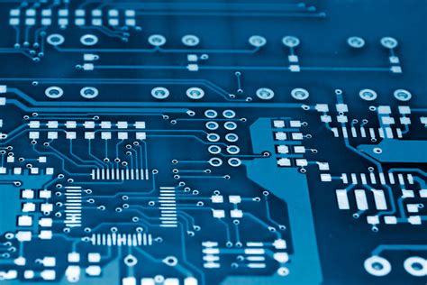
custom printed circuit board (PCB) assembly
Custom PCB assembly is the process of designing and manufacturing printed circuit boards
(PCBs) to meet specific customer requirements. The PCB is an essential component of
electronic devices, and it plays a crucial role in the overall functionality of the device.
PCBs are used in a wide range of applications, including consumer electronics, medical
devices, aerospace, and defense systems.
The custom PCB assembly process involves several steps, including design, prototyping,
testing, and production. The first step in the process is the design phase, where the
customer provides the specifications for the PCB. The design team then creates a schematic
diagram and a layout of the PCB, which is used to manufacture the physical board.

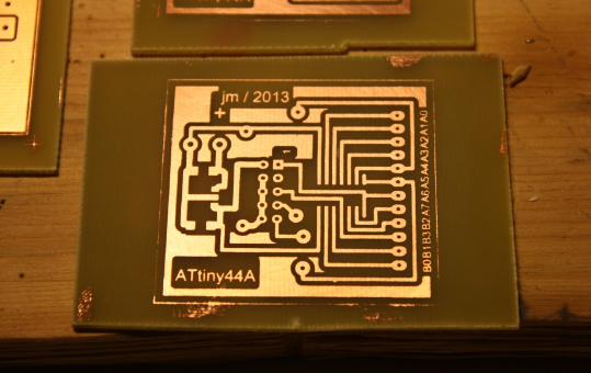
Once the design is complete, the next step is prototyping. This involves creating a small
batch of PCBs to test for functionality and performance. The prototype is tested to ensure
that it meets the customer’s requirements and specifications. If any issues are identified,
the design is modified, and a new prototype is created.
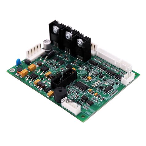
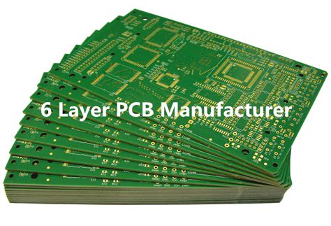
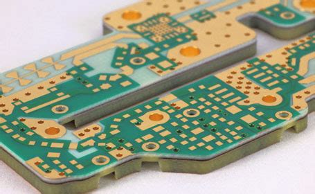
Once the prototype has been approved, the PCB assembly process moves into the production
phase. The production phase involves the mass production of the PCBs. The PCBs are
manufactured using a variety of techniques, including surface mount technology (SMT) and
through-hole technology (THT).
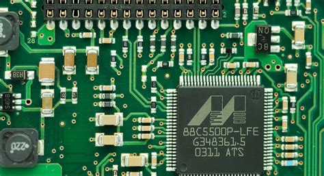
SMT is a popular technique used in PCB assembly, where components are mounted directly onto
the surface of the board. This technique is ideal for small, compact devices that require a
high level of precision. THT, on the other hand, involves mounting components through holes
in the board. This technique is ideal for larger, more complex devices that require a
higher level of durability.
R4VRM")
Once the PCBs have been manufactured, they are tested to ensure that they meet the
customer’s specifications. This involves a series of tests, including functional testing,
electrical testing, and environmental testing. Functional testing involves testing the PCB
to ensure that it performs as expected. Electrical testing involves testing the electrical
properties of the PCB, such as voltage and current. Environmental testing involves testing
the PCB’s resistance to various environmental factors, such as temperature and humidity.
Custom PCB assembly offers several benefits over standard PCBs. Custom PCBs are designed to
meet specific customer requirements, which means that they are tailored to the customer’s
needs. This results in a higher level of performance and functionality, which can improve
the overall performance of the device. Custom PCBs are also more durable and reliable,
which reduces the risk of failure and downtime.

In conclusion, custom PCB assembly is a critical process in the manufacturing of electronic
devices. It involves designing and manufacturing PCBs to meet specific customer
requirements, which results in a higher level of performance and functionality. Custom PCBs
are also more durable and reliable, which reduces the risk of failure and downtime. If you
are looking to manufacture electronic devices, custom PCB assembly is a process that you
should consider.