Design considerations for high frequency pcb winding magnetic components
Material Selection For High-Frequency PCB Winding Magnetic Components
When designing high-frequency PCB winding magnetic components, material selection plays a pivotal role in determining the performance, efficiency, and reliability of the final product. The choice of materials directly influences the magnetic properties, thermal management, and overall durability of the components. Therefore, understanding the characteristics and implications of different materials is essential for engineers and designers working in this field.
To begin with, the core material is a critical consideration.
Ferrite cores are commonly used in high-frequency applications due to their high magnetic permeability and low electrical conductivity, which help minimize eddy current losses. These materials are particularly advantageous in applications operating at frequencies ranging from a few kilohertz to several megahertz. However, for even higher frequency applications, such as those exceeding 10 MHz, powdered iron cores may be preferred. These cores offer lower core losses at high frequencies, albeit at the expense of reduced permeability compared to ferrites.
In addition to core materials, the selection of winding materials is equally important.
Copper is the most prevalent choice for winding due to its excellent electrical conductivity, which minimizes resistive losses. However, at high frequencies, the skin effect becomes significant, causing current to flow primarily on the surface of the conductor. To mitigate this, designers often use Litz wire, which consists of multiple thin strands of insulated wire twisted together. This configuration reduces skin effect losses and improves the efficiency of the magnetic component.
Moreover, the choice of dielectric materials for the PCB substrate is crucial.
High-frequency applications demand substrates with low dielectric loss and stable dielectric constant to ensure signal integrity and minimize energy dissipation. Materials such as polytetrafluoroethylene (PTFE) and ceramic-filled laminates are popular choices due to their favorable electrical properties. These materials help maintain consistent performance across a wide frequency range, which is essential for high-frequency magnetic components.
Thermal management is another critical aspect influenced by material selection.
High-frequency operations often generate significant heat, which can degrade performance and reliability if not properly managed. Therefore, materials with good thermal conductivity are essential to dissipate heat effectively. For instance, using substrates with embedded metal layers or incorporating thermal vias can enhance heat dissipation. Additionally, selecting core materials with high Curie temperatures ensures that the magnetic properties remain stable under elevated temperatures.
Furthermore, mechanical considerations should not be overlooked.
The materials chosen must withstand the mechanical stresses encountered during manufacturing and operation. This includes resistance to thermal expansion, which can cause mechanical failure or misalignment of components. Therefore, materials with compatible coefficients of thermal expansion are preferred to ensure structural integrity.
In conclusion, the selection of materials for high-frequency PCB winding magnetic components is a multifaceted process that requires careful consideration of various factors. From core and winding materials to dielectric substrates and thermal management solutions, each choice impacts the performance and reliability of the final product. By understanding the properties and trade-offs of different materials, designers can optimize their designs to meet the demanding requirements of high-frequency applications. This comprehensive approach ensures that the magnetic components not only perform efficiently but also maintain their integrity over the intended lifespan.
Thermal Management Strategies In High-Frequency PCB Designs
In the realm of high-frequency PCB designs, thermal management emerges as a critical consideration, particularly when dealing with winding magnetic components. As electronic devices continue to shrink in size while increasing in functionality, the demand for efficient thermal management strategies becomes paramount. The heat generated by high-frequency operations can significantly impact the performance and reliability of PCB components, necessitating a comprehensive approach to thermal management.
To begin with, understanding the sources of heat generation in high-frequency PCB designs is essential.
Winding magnetic components, such as inductors and transformers, are often at the heart of these designs. These components can generate substantial heat due to core losses, copper losses, and eddy currents. As the frequency of operation increases, these losses tend to escalate, making effective thermal management indispensable. Therefore, designers must consider both the material properties and the physical layout of these components to mitigate heat generation.
One of the primary strategies for managing heat in high-frequency PCB designs is the selection of appropriate materials.
High thermal conductivity materials, such as certain ceramics or metal composites, can be employed to facilitate efficient heat dissipation. Additionally, the use of low-loss core materials in magnetic components can reduce core losses, thereby minimizing heat generation. By carefully selecting materials that offer both electrical performance and thermal efficiency, designers can address one of the fundamental challenges in high-frequency PCB design.
Moreover, the physical layout of the PCB plays a crucial role in thermal management.
Effective layout design can enhance heat dissipation and prevent hotspots from forming. For instance, increasing the surface area of the PCB can improve heat dissipation by allowing more efficient airflow. Additionally, strategic placement of components can help distribute heat more evenly across the board. By positioning high-heat-generating components away from sensitive areas, designers can prevent localized overheating and ensure the overall stability of the PCB.
Furthermore, incorporating thermal vias and heat sinks into the PCB design can significantly enhance thermal management.
Thermal vias are small holes filled with conductive material that connect different layers of the PCB, allowing heat to be transferred away from critical components. Heat sinks, on the other hand, are external devices attached to the PCB to dissipate heat into the surrounding environment. By integrating these elements into the design, engineers can effectively manage the thermal load and maintain optimal operating temperatures.
In addition to these strategies, active cooling methods may also be considered for high-frequency PCB designs.
While passive cooling techniques, such as those mentioned above, are often sufficient, active cooling can provide an additional layer of thermal management. This may involve the use of fans or liquid cooling systems to actively remove heat from the PCB. Although these methods can be more complex and costly, they offer a viable solution for designs where passive cooling is inadequate.
In conclusion, thermal management in high-frequency PCB designs is a multifaceted challenge that requires careful consideration of materials, layout, and cooling techniques. By understanding the sources of heat generation and implementing effective strategies, designers can ensure the reliability and performance of their PCB components. As technology continues to advance, the importance of robust thermal management in high-frequency applications will only grow, making it a critical area of focus for engineers and designers alike.
Minimizing Parasitic Effects In High-Frequency Magnetic Components
In the realm of high-frequency magnetic components, particularly those involving printed circuit board (PCB) winding, minimizing parasitic effects is a critical design consideration. These parasitic elements, which include parasitic capacitance and inductance, can significantly impact the performance and efficiency of magnetic components, leading to undesirable effects such as increased losses, reduced bandwidth, and potential instability. Therefore, understanding and mitigating these parasitic effects is essential for optimizing the functionality of high-frequency magnetic components.
To begin with, parasitic capacitance arises from the proximity of conductive elements within the PCB layout.
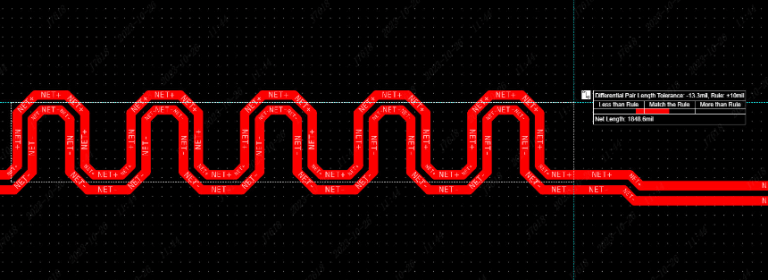
In high-frequency applications, the electric fields between these conductors can lead to unintended capacitive coupling. This effect is particularly pronounced in multilayer PCBs where the close spacing of layers can exacerbate capacitive interactions. To minimize parasitic capacitance, designers can employ strategies such as increasing the spacing between conductive traces and layers, using thinner dielectric materials, and implementing ground planes to shield sensitive areas. Additionally, careful routing of traces to avoid unnecessary overlaps and intersections can further reduce capacitive coupling.
In parallel, parasitic inductance is another critical factor that can degrade the performance of high-frequency magnetic components.
This inductance is primarily associated with the loop areas formed by current paths within the PCB. Larger loop areas result in higher inductive effects, which can lead to increased impedance and reduced efficiency. To mitigate parasitic inductance, designers should focus on minimizing loop areas by keeping current paths as short and direct as possible. Employing techniques such as using multiple vias to connect layers and optimizing the placement of components can also help in reducing inductive effects.
Moreover, the choice of materials plays a significant role in minimizing parasitic effects.
High-frequency applications benefit from materials with low dielectric constants and low loss tangents, as these properties help reduce both capacitive and inductive parasitics. Advanced materials such as PTFE-based laminates or ceramic-filled substrates are often preferred for their superior electrical characteristics. Furthermore, the surface finish of the PCB can influence parasitic effects, with smoother finishes generally offering lower losses and better high-frequency performance.
Transitioning to the aspect of simulation and modeling, these tools are indispensable in the design process for high-frequency magnetic components.
By employing electromagnetic simulation software, designers can predict and analyze parasitic effects before physical prototyping. This approach allows for the identification of potential issues and the evaluation of different design strategies to mitigate parasitics effectively. Simulation also provides insights into the interactions between various components and the overall system, enabling more informed design decisions.
In addition to simulation, prototyping and testing remain crucial in the design process.
Despite the accuracy of simulations, real-world testing is necessary to validate the performance of the designed components. By measuring parameters such as impedance, insertion loss, and return loss, designers can assess the impact of parasitic effects and make necessary adjustments. Iterative testing and refinement ensure that the final design meets the desired specifications and performance criteria.
In conclusion, minimizing parasitic effects in high-frequency PCB winding magnetic components is a multifaceted challenge that requires careful consideration of layout, materials, simulation, and testing.
By addressing these factors, designers can enhance the performance and reliability of magnetic components, ultimately leading to more efficient and effective high-frequency applications. Through a combination of strategic design practices and advanced tools, the impact of parasitic elements can be significantly reduced, paving the way for innovative solutions in the field of high-frequency magnetics.
Layout Techniques For Optimizing High-Frequency PCB Winding Performance
In the realm of high-frequency applications, the design of printed circuit board (PCB) winding magnetic components is a critical factor that significantly influences performance. As frequencies increase, the challenges associated with PCB winding design become more pronounced, necessitating meticulous attention to layout techniques. To optimize high-frequency PCB winding performance, several key considerations must be addressed, each contributing to the overall efficiency and functionality of the magnetic components.
Firstly, the choice of materials plays a pivotal role in high-frequency applications.
Selecting materials with low dielectric losses and high thermal conductivity is essential to minimize energy dissipation and manage heat effectively. Copper is often the preferred choice for windings due to its excellent electrical conductivity, which reduces resistive losses. However, the thickness of the copper traces must be carefully considered to balance current-carrying capacity with skin effect, a phenomenon where alternating current tends to flow near the surface of the conductor at high frequencies. By optimizing trace thickness, designers can mitigate skin effect losses and enhance performance.
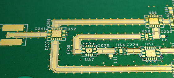
Moreover, the geometric configuration of the windings is another crucial aspect.
Spiral and planar winding designs are commonly employed in high-frequency PCB applications. Spiral windings offer compactness and ease of integration, while planar windings provide better thermal management and reduced parasitic inductance. The choice between these configurations depends on the specific application requirements, including space constraints and thermal considerations. Additionally, the spacing between windings should be optimized to minimize parasitic capacitance, which can adversely affect performance at high frequencies.
Transitioning to the topic of electromagnetic interference (EMI), it is imperative to implement effective shielding and grounding techniques.
High-frequency PCB winding components are susceptible to EMI, which can degrade signal integrity and lead to performance issues. To combat this, designers should incorporate ground planes and shielding layers within the PCB layout. Ground planes help to provide a low-impedance path for return currents, thereby reducing EMI. Shielding layers, on the other hand, can be used to isolate sensitive components from external electromagnetic fields, ensuring stable operation.
Furthermore, thermal management is a critical consideration in high-frequency PCB winding design.
As frequencies increase, so does the potential for heat generation, which can impact the reliability and longevity of the components. Effective thermal management strategies, such as the use of thermal vias and heat sinks, are essential to dissipate heat efficiently. Thermal vias facilitate heat transfer from the PCB surface to the inner layers, while heat sinks provide a means to dissipate heat into the surrounding environment. By implementing these techniques, designers can ensure that the components operate within safe temperature limits.
In addition to these considerations, simulation and modeling tools are invaluable in the design process
.Advanced simulation software allows designers to predict the behavior of high-frequency PCB winding components under various conditions, enabling them to make informed decisions about layout and material choices. By leveraging these tools, potential issues can be identified and addressed early in the design phase, reducing the likelihood of costly revisions later on.
In conclusion, optimizing high-frequency PCB winding performance requires a comprehensive approach that encompasses material selection, geometric configuration, EMI mitigation, thermal management, and the use of simulation tools. By carefully considering each of these factors, designers can create high-frequency PCB winding magnetic components that deliver superior performance and reliability in demanding applications. Through meticulous design and layout techniques, the challenges associated with high-frequency operation can be effectively managed, paving the way for innovative solutions in the ever-evolving field of electronics.