Design Considerations for High-Frequency PCB Winding Magnetic Components
Abstract
This paper explores the critical design considerations for implementing magnetic components (inductors and transformers) using printed circuit board (PCB) windings in high-frequency power electronics applications. As switching frequencies continue to increase in modern power conversion systems—reaching into the MHz range—traditional wire-wound magnetic components face significant challenges related to skin and proximity effects, parasitic capacitance, and thermal management. PCB-embedded magnetics offer numerous advantages including precise control over winding geometry, excellent repeatability, and compatibility with automated assembly processes. This article systematically examines key design factors including winding layout optimization, core selection, loss mechanisms, thermal considerations, and electromagnetic interference (EMI) mitigation strategies specific to high-frequency operation. Practical design guidelines and trade-offs are discussed to help engineers implement effective PCB-based magnetic components in high-frequency applications.
1. Introduction
The ongoing trend toward higher switching frequencies in power electronics—driven by demands for increased power density, faster transient response, and reduced passive component size—has created both opportunities and challenges for magnetic component design. While increasing frequency allows for smaller energy storage requirements (E = ½LI²), it also exacerbates high-frequency losses and parasitic effects that can dominate component performance.
PCB-wound magnetic components have emerged as a compelling solution for frequencies ranging from hundreds of kHz to several MHz. Unlike conventional wire-wound designs, PCB implementations offer:
- Precise control over conductor geometry and spacing
- Excellent inter-winding capacitance management
- Repeatable manufacturing with tight tolerances
- Direct integration with power circuitry
- Improved thermal paths through the PCB
However, realizing these advantages requires careful attention to numerous design factors that become increasingly critical at high frequencies.
2. Winding Layout Design
2.1 Conductor Thickness and Skin Effect
At high frequencies, current tends to flow near the surface of conductors due to the skin effect. The skin depth (δ) is given by:
δ = √(ρ/πμf)
Where:
ρ = resistivity of conductor (Ω·m)
μ = permeability (H/m)
f = frequency (Hz)
For copper at 1MHz, δ ≈ 66μm. This implies:
- Conductors thicker than ~2δ (132μm for 1MHz) will have underutilized cross-sections
- Standard 1oz (35μm) and 2oz (70μm) copper are generally appropriate up to several MHz
- Thicker copper may require special etching techniques or segmented designs
2.2 Winding Patterns
Common PCB winding configurations include:
Spiral Windings:
- Concentric square or circular turns
- Simple to implement but exhibit non-uniform current distribution
- Significant inter-turn capacitance
Meander (Serpentine) Windings:
- Alternating direction traces
- More uniform current distribution
- Lower inter-turn capacitance than spirals
Interleaved Windings:
- Primary and secondary traces alternated in layers
- Reduces leakage inductance
- Improves coupling but increases inter-winding capacitance
2.3 Multi-Layer Considerations
Optimal layer utilization depends on:
- Via Placement: Minimize via count to reduce resistance, but ensure proper current sharing
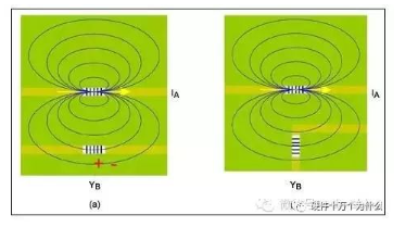
- Layer Stacking: Adjacent layers should carry opposing currents to cancel magnetic fields
- Inter-layer Insulation: Thin dielectrics improve coupling but increase capacitance
3. Core Selection and Integration
3.1 Core Material Properties
Key material parameters for high-frequency operation:
- Permeability (μ): High initial μ is less critical at high frequencies due to roll-off
- Resistivity (ρ): Ferrites (ρ ≈ 1-100 Ω·m) outperform laminated metals at MHz frequencies
- Curie Temperature: Must exceed maximum operating temperature
- Loss Tangent: Core losses (hysteresis + eddy current) dominate at high frequency
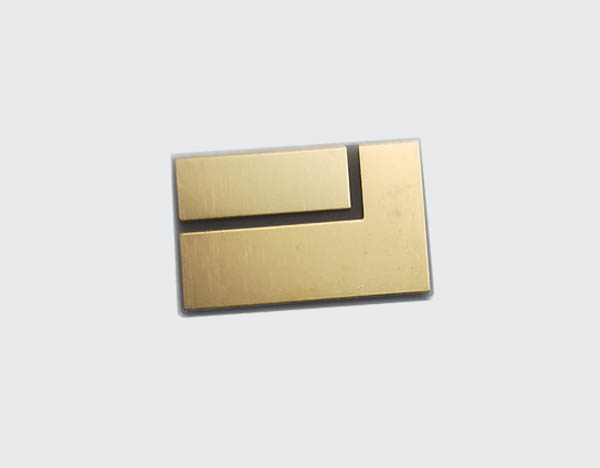
3.2 Core Geometries for PCB Integration
Common configurations:
- Planar E Cores: Allow winding window between core halves
- Pot Cores: Provide excellent shielding but challenging to assemble
- Printed Magnetics: Deposited magnetic materials enable fully integrated solutions
3.3 Air Gap Considerations
Intentional air gaps:
- Reduce effective permeability
- Prevent saturation but increase fringing fields
- May require distributed gaps in high-frequency designs
4. Loss Mechanisms and Mitigation
4.1 Conductor Losses
Total conductor losses include:
P_conductor = P_DC + P_skin + P_proximity
Mitigation strategies:
- Litz-like PCB Patterns: Multiple parallel thin traces
- Transposed Windings: Rotate conductor positions between layers
- Optimal Width-Spacing Ratios: Typically 1:1 to 3:1 trace width to spacing
4.2 Core Losses
Core loss can be estimated using the Steinmetz equation:
P_v = kf^αB^β
Where k, α, β are material parameters.
High-frequency strategies:
- Use low-loss ferrite materials specifically formulated for MHz operation
- Operate at lower flux density (B) when possible
- Consider distributed gap structures
4.3 Parasitic Capacitance
Inter-winding capacitance causes:
- Resonant peaks in impedance characteristics
- Common-mode noise propagation
- Increased EMI
Reduction techniques:
- Electrostatic Shields: Thin copper layers between windings
- Increased Inter-winding Spacing: At least 3× dielectric thickness
- Balanced Winding Structures: Symmetrical layouts to cancel capacitive coupling
5. Thermal Management
High-frequency operation leads to increased loss densities. PCB magnetics benefit from:
- Thermal Vias: Connect hot spots to internal or backside copper layers
- Exposed Copper: Remove solder mask over traces for better heat dissipation
- Core Attachment: Thermally conductive adhesives for core-to-PCB interface
- Copper Thickness: Thicker copper improves both conduction and heat spreading
6. EMI Considerations
High di/dt in windings generates:
- Radiated emissions from loop areas
- Conducted noise through parasitic capacitances
Mitigation approaches:
- Minimize Loop Areas: Tight winding layouts
- Twisted Virtual Geometries: Opposite current directions in adjacent layers
- Shielding: Copper pours around windings connected to appropriate potentials
- Balanced Designs: Differential winding structures where applicable
7. Practical Design Guidelines
- Frequency-Specific Optimization:
- Below 500kHz: Traditional designs often suffice
- 500kHz-3MHz: Require careful attention to skin/proximity effects
- Above 3MHz: May need specialized approaches like litz-like patterns
- Winding Layout Rules:
- Keep dI/dt loops small
- Maintain symmetry in differential designs
- Use 45° corners rather than 90° to reduce crowding effects
- Material Selection:
- FR4 is acceptable up to ~5MHz
- High-frequency laminates (Rogers, Isola) for >10MHz
- Low-profile copper (≤2oz) for MHz operation
- Manufacturing Considerations:
- Specify tight etching tolerances (±10% or better)
- Control dielectric thickness between layers
- Consider via filling for high-current paths
8. Future Trends
Emerging developments in PCB magnetics include:
- Embedded Thin-Film Magnetics: Deposited magnetic materials between layers
- 3D-Printed Additive Structures: Enabling complex 3D winding geometries
- Active Integrated Magnetics: Combining semiconductor devices within magnetic structures
- Meta-material Inspired Designs: Engineered permeability distributions
9. Conclusion
Designing high-frequency PCB-wound magnetic components requires a multidisciplinary approach considering electromagnetic, thermal, and manufacturing constraints. By carefully optimizing winding layouts, core integration, and loss mitigation strategies, engineers can realize the full benefits of PCB-based magnetics in high-frequency applications. As switching frequencies continue to rise and power densities increase, these techniques will become increasingly essential for next-generation power electronics systems.
The key to successful implementation lies in understanding the frequency-dependent behaviors of all component aspects and making appropriate trade-offs between conflicting requirements. With proper design, PCB-wound magnetics can offer superior performance compared to conventional approaches in the MHz frequency range and beyond.