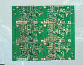
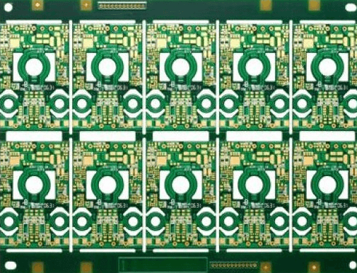
Design high speed pcb
Best Practices For High Speed PCB Layout
Design high speed PCB is a complex task that requires meticulous attention to detail and a deep understanding of both electrical and mechanical principles.
As technology advances, the demand for faster and more efficient electronic devices continues to grow, making the need for high-speed PCB design more critical than ever. To achieve optimal performance, it is essential to follow best practices that ensure signal integrity, minimize electromagnetic interference (EMI), and maintain overall system reliability.
One of the fundamental aspects of high-speed PCB design is the careful management of signal integrity.
High-speed signals are susceptible to various forms of degradation, such as reflection, crosstalk, and attenuation. To mitigate these issues, it is crucial to maintain consistent impedance throughout the signal paths.
This can be achieved by using controlled impedance traces, which involve precise calculations of trace width, spacing, and the dielectric properties of the PCB material. Additionally, differential signaling can be employed to reduce noise and improve signal quality, especially in high-speed data transmission applications.
Transitioning to the topic of layout, the placement of components plays a significant role in the performance of a high-speed PCB.
Components should be strategically positioned to minimize the length of high-speed signal paths and reduce the potential for signal degradation. Placing critical components, such as processors and memory modules, close to each other can help achieve this goal. Furthermore, it is advisable to keep high-speed signal traces away from noisy components, such as power supplies and oscillators, to prevent interference.
Another important consideration is the use of proper grounding techniques.
A solid ground plane is essential for providing a low-impedance return path for high-speed signals, which helps to reduce EMI and improve signal integrity. It is recommended to use a multi-layer PCB design, with at least one dedicated ground plane layer. This not only enhances grounding but also allows for better separation of signal and power planes, further reducing the risk of interference.
In addition to grounding, power distribution is a critical factor in high-speed PCB design.
Ensuring a stable and clean power supply is vital for the reliable operation of high-speed circuits. Decoupling capacitors should be placed close to the power pins of integrated circuits to filter out noise and provide a stable voltage. Using multiple power planes can also help to distribute power more evenly and reduce voltage drops across the PCB.
Thermal management is another key aspect that cannot be overlooked.
High-speed components often generate significant amounts of heat, which can affect performance and reliability if not properly managed. Effective thermal management techniques, such as the use of thermal vias, heat sinks, and proper airflow design, are essential to dissipate heat and maintain optimal operating temperatures.
Lastly, it is important to consider the manufacturability of the high-speed PCB design.
While advanced design techniques are necessary for high-speed performance, they should not compromise the ease of manufacturing. Collaborating with PCB manufacturers early in the design process can help identify potential issues and ensure that the design is both high-performing and manufacturable.
In conclusion, designing high-speed PCBs requires a comprehensive approach that encompasses signal integrity, component placement, grounding, power distribution, thermal management, and manufacturability. By adhering to these best practices, designers can create high-speed PCBs that meet the demands of modern electronic devices, ensuring reliable and efficient performance.
Signal Integrity Considerations In High Speed PCB Design
In the realm of high-speed PCB design, signal integrity considerations are paramount to ensuring optimal performance and reliability. As electronic devices continue to evolve, the demand for faster data transmission rates and higher processing speeds has necessitated a meticulous approach to PCB design. Signal integrity, which refers to the quality and reliability of electrical signals as they travel through a circuit, becomes increasingly critical as clock speeds and data rates escalate.
One of the primary factors affecting signal integrity in high-speed PCB design is impedance control.
Impedance mismatches can lead to signal reflections, which in turn cause data corruption and timing errors. To mitigate this, designers must carefully calculate and control the impedance of transmission lines. This involves selecting appropriate materials, layer stack-ups, and trace geometries. For instance, using differential pairs for high-speed signals can help maintain consistent impedance and reduce electromagnetic interference (EMI).
Moreover, crosstalk is another significant concern in high-speed PCB design.
Crosstalk occurs when a signal in one trace induces unwanted noise in an adjacent trace, potentially leading to data errors. To minimize crosstalk, designers should maintain adequate spacing between traces and employ shielding techniques. Ground planes and guard traces can be particularly effective in isolating high-speed signals and reducing interference. Additionally, routing high-speed signals on internal layers, sandwiched between ground planes, can further enhance signal integrity by providing a controlled impedance environment.
Transitioning to the topic of signal attenuation, it is essential to recognize that high-frequency signals are more susceptible to losses as they propagate through PCB materials.
These losses, known as dielectric and conductor losses, can degrade signal quality and limit the effective transmission distance. To address this, designers should select low-loss dielectric materials and optimize trace widths and thicknesses. Furthermore, minimizing the number of vias and connectors in the signal path can help reduce signal degradation.
Another critical aspect of signal integrity in high-speed PCB design is managing power distribution.
Power integrity issues, such as voltage drops and ground bounce, can adversely affect signal quality. To ensure stable power delivery, designers should implement robust power distribution networks (PDNs) with low impedance paths. Decoupling capacitors, strategically placed near high-speed components, can help filter out noise and provide a stable power supply. Additionally, using multiple ground and power planes can enhance the overall performance of the PDN.
As we delve deeper into the intricacies of high-speed PCB design, it becomes evident that careful consideration of signal return paths is crucial.
High-speed signals generate return currents that follow the path of least impedance, typically through the ground plane. Interruptions in the return path, such as gaps in the ground plane or improper via placement, can lead to signal integrity issues. Ensuring continuous and unbroken return paths by maintaining solid ground planes and strategically placing vias can significantly improve signal quality.
In conclusion, signal integrity considerations are integral to the success of high-speed PCB design. By meticulously controlling impedance, minimizing crosstalk, addressing signal attenuation, managing power distribution, and ensuring proper signal return paths, designers can achieve reliable and high-performance PCBs. As technology continues to advance, the importance of signal integrity in high-speed PCB design will only grow, necessitating ongoing innovation and attention to detail in the design process.
Techniques For Reducing EMI In High Speed PCBs
Designing high-speed printed circuit boards (PCBs) presents a unique set of challenges, particularly when it comes to managing electromagnetic interference (EMI). As electronic devices become more sophisticated and operate at higher frequencies, the potential for EMI increases, which can degrade performance and lead to compliance issues. Therefore, implementing effective techniques to reduce EMI is crucial for the success of high-speed PCB designs.
One of the primary techniques for reducing EMI in high-speed PCBs is proper grounding.
A well-designed ground plane can significantly mitigate EMI by providing a low-impedance path for return currents. Ensuring that the ground plane is continuous and unbroken is essential, as any gaps can create loops that act as antennas, radiating unwanted electromagnetic energy. Additionally, using multiple ground planes in a multilayer PCB can further enhance EMI suppression by providing additional shielding and reducing the inductance of return paths.
Another critical aspect of EMI reduction is the careful routing of high-speed signals.
Signal traces should be kept as short and direct as possible to minimize the loop area, which in turn reduces the potential for radiated emissions. When routing differential pairs, maintaining consistent spacing and minimizing skew between the traces is vital to ensure that the signals remain balanced, thereby reducing common-mode noise. Furthermore, avoiding right-angle bends in traces can help prevent reflections and impedance discontinuities, which can contribute to EMI.
Decoupling capacitors play a significant role in managing EMI by stabilizing the power supply and filtering out high-frequency noise.
Placing these capacitors as close as possible to the power pins of integrated circuits (ICs) is crucial for their effectiveness. Using a combination of capacitors with different values can provide a broader frequency range of noise suppression. Additionally, employing a power distribution network (PDN) with low impedance across a wide frequency range can help maintain a stable power supply, further reducing EMI.
Shielding is another effective technique for EMI reduction in high-speed PCBs.
By enclosing sensitive components or entire sections of the PCB in a conductive shield, it is possible to block electromagnetic fields from entering or leaving the shielded area. This can be particularly useful for protecting analog circuits from digital noise or preventing high-speed signals from radiating EMI. However, it is essential to ensure that the shield is properly grounded to avoid creating additional EMI issues.
The use of controlled impedance traces is also crucial in high-speed PCB design.
By carefully designing the trace width, spacing, and dielectric material, it is possible to maintain a consistent impedance, which helps to minimize signal reflections and crosstalk. This not only improves signal integrity but also reduces the potential for EMI. Additionally, employing techniques such as microstrip or stripline routing can provide better control over impedance and further enhance EMI performance.
Finally, conducting thorough simulations and testing during the design process is essential for identifying and mitigating potential EMI issues.
Tools such as electromagnetic compatibility (EMC) simulation software can help predict how a PCB will behave in terms of EMI and allow designers to make necessary adjustments before fabrication. Once the PCB is manufactured, performing EMI testing in a controlled environment can validate the design and ensure compliance with relevant standards.
In conclusion, reducing EMI in high-speed PCBs requires a multifaceted approach that includes proper grounding, careful signal routing, effective use of decoupling capacitors, shielding, controlled impedance traces, and thorough testing. By implementing these techniques, designers can create high-speed PCBs that not only perform reliably but also meet stringent EMI requirements, ensuring the success of their electronic products.
Material Selection For High Speed PCB Applications
When designing high-speed printed circuit boards (PCBs), the selection of materials plays a pivotal role in ensuring optimal performance and reliability. The choice of substrate, dielectric materials, and copper cladding can significantly impact signal integrity, thermal management, and overall functionality. Therefore, understanding the properties and implications of various materials is essential for engineers and designers working on high-speed PCB applications.
To begin with, the substrate material forms the foundation of the PCB and must be chosen with care.
FR-4, a widely used substrate, is often the default choice due to its cost-effectiveness and satisfactory performance in many applications. However, for high-speed designs, FR-4 may not always be suitable due to its relatively high dielectric constant (Dk) and loss tangent (Df). These properties can lead to signal degradation and increased electromagnetic interference (EMI) at higher frequencies. Consequently, alternative materials such as Rogers, Taconic, and Isola, which offer lower Dk and Df values, are frequently considered. These materials provide better signal integrity and reduced signal loss, making them ideal for high-speed applications.
In addition to the substrate, the dielectric material between the layers of the PCB is crucial.
The dielectric constant of the material affects the impedance of the transmission lines, which in turn influences signal speed and integrity. Materials with a low dielectric constant are preferred for high-speed designs as they allow for faster signal propagation and reduced signal distortion. Furthermore, the loss tangent of the dielectric material determines how much signal power is lost as heat. A lower loss tangent is desirable to minimize signal attenuation and maintain signal strength over longer distances.
Another important consideration is the copper cladding used in the PCB.
The thickness and quality of the copper can affect the board’s ability to handle high-frequency signals. Thicker copper layers can carry more current and dissipate heat more effectively, which is beneficial for high-speed applications that generate significant thermal loads. However, thicker copper can also increase the board’s overall thickness and potentially complicate the manufacturing process. Therefore, a balance must be struck between thermal management and manufacturability.
Thermal management is another critical aspect of material selection for high-speed PCBs. High-speed circuits often generate substantial heat, which can affect performance and reliability if not properly managed. Materials with high thermal conductivity, such as certain ceramics or metal-core substrates, can help dissipate heat more efficiently. Additionally, incorporating thermal vias and heat sinks into the design can further enhance thermal management and ensure the longevity of the PCB.
Moreover, the coefficient of thermal expansion (CTE) of the materials used must be compatible with the components mounted on the PCB. Mismatched CTEs can lead to mechanical stress and potential failure of solder joints, especially in high-speed applications where thermal cycling is common. Selecting materials with similar CTEs helps maintain structural integrity and reliability over the board’s operational life.
In conclusion, material selection for high-speed PCB applications is a multifaceted process that requires careful consideration of various factors, including dielectric properties, thermal management, and mechanical compatibility. By choosing the appropriate materials, designers can enhance signal integrity, reduce EMI, and ensure the overall reliability of high-speed PCBs. As technology continues to advance and the demand for faster, more efficient electronic devices grows, the importance of meticulous material selection in PCB design cannot be overstated.