Design of PCB-Based Small Antennas for Modern Wireless Applications
Abstract
The rapid advancement of wireless communication systems has necessitated the development of compact, efficient, and low-cost antennas. Printed circuit board (PCB)-based small antennas have emerged as a viable solution due to their ease of integration, lightweight structure, and compatibility with modern electronic devices. This paper discusses the fundamental design considerations, performance parameters, and implementation techniques for PCB-based small antennas. Various antenna topologies, including microstrip patches, planar inverted-F antennas (PIFAs), and meandered monopoles, are analyzed in terms of their radiation characteristics, impedance matching, and miniaturization strategies. Furthermore, the impact of substrate materials, feeding techniques, and geometrical optimizations on antenna performance is explored. Finally, practical applications and future trends in PCB antenna design are highlighted.
1. Introduction
With the increasing demand for wireless connectivity in applications such as IoT, 5G, wearable devices, and RFID, the need for compact and high-performance antennas has grown significantly. Traditional antennas, such as dipoles and helical structures, often occupy large volumes, making them unsuitable for modern miniaturized electronics. PCB-based antennas offer an attractive alternative due to their planar structure, low profile, and compatibility with standard fabrication processes.
Small antennas, typically defined as those with dimensions much smaller than the operating wavelength, face inherent challenges such as low radiation efficiency, narrow bandwidth, and poor gain. However, careful design and optimization can mitigate these limitations. This paper focuses on the design methodologies and performance enhancements of PCB-based small antennas.
2. Fundamental Design Considerations
2.1 Antenna Miniaturization Techniques
Miniaturization is a critical aspect of small antenna design. Common techniques include:
- Meandering and folding: Increasing the electrical length by bending the conductor.
- High-permittivity substrates: Using dielectric materials with high εr to reduce the guided wavelength.
- Slot loading: Introducing slots or defects to perturb current distribution and lower resonance frequency.
- Capacitive and inductive loading: Adding lumped elements to adjust impedance and resonance.
2.2 Substrate Selection
The choice of PCB substrate significantly affects antenna performance. Key parameters include:
- Dielectric constant (εr): Higher εr allows for smaller antenna dimensions but may reduce bandwidth.
- Loss tangent (tanδ): Lower tanδ minimizes dielectric losses, improving efficiency.
- Thickness: Thicker substrates enhance bandwidth but may increase surface wave losses.
Common substrates include FR-4 (εr ≈ 4.3, tanδ ≈ 0.02), Rogers RO4003C (εr ≈ 3.38, tanδ ≈ 0.0027), and ceramic-filled PTFE (εr ≈ 10.2).
2.3 Feeding Techniques
Proper impedance matching is crucial for maximizing power transfer. Common feeding methods include:
- Microstrip line feed: Simple and widely used but may introduce spurious radiation.
- Coaxial probe feed: Provides good impedance matching but requires soldering.
- Coupling-based feeds (e.g., aperture coupling): Reduces interference but increases complexity.
3. PCB-Based Small Antenna Topologies
3.1 Microstrip Patch Antennas
Microstrip patch antennas consist of a radiating patch on a grounded dielectric substrate. They offer advantages such as low profile, ease of fabrication, and compatibility with array configurations. However, their relatively large size at lower frequencies limits their use in compact devices. Miniaturization techniques include:
- Shorting pins or walls: Reduces resonant frequency.
- Slotted patches: Introduces additional resonance modes.
- Stacked patches: Enhances bandwidth.
3.2 Planar Inverted-F Antennas (PIFAs)
PIFAs are popular in mobile devices due to their compact size and good impedance matching. They consist of a shorted radiating patch, reducing the antenna’s height while maintaining a quarter-wavelength resonance. Design considerations include:
- Ground plane effects: Performance depends on the ground plane size.
- Tuning stubs: Adjust resonance frequency and bandwidth.
- Multi-band operation: Using multiple branches or parasitic elements.
3.3 Meandered Monopoles
Meandered monopoles extend the current path within a limited area, enabling size reduction. They are suitable for applications requiring omnidirectional radiation. Challenges include:
- Increased ohmic losses due to conductor length.
- Trade-off between miniaturization and bandwidth.
- Sensitivity to nearby components.
4. Performance Optimization Strategies
4.1 Impedance Matching
Matching networks (e.g., L-sections, stubs) can improve return loss. Advanced techniques include:
- Genetic algorithms for geometry optimization.
- Defected ground structures (DGS) to enhance bandwidth.
- Reconfigurable matching circuits for multi-band operation.
4.2 Radiation Efficiency Enhancement
- Minimizing dielectric and conductor losses.
- Using electromagnetic bandgap (EBG) structures to suppress surface waves.
- Employing parasitic elements for gain improvement.
4.3 Multi-Band and Wideband Design
- Fractal geometries for multi-resonance behavior.
- Log-periodic or tapered structures for wideband operation.
- Frequency-reconfigurable antennas using PIN diodes or MEMS switches.
5. Practical Applications
PCB-based small antennas are widely used in:
- Smartphones and tablets (PIFAs, MIMO configurations).
- Wearable electronics (flexible PCB antennas).
- IoT sensors (compact printed monopoles).
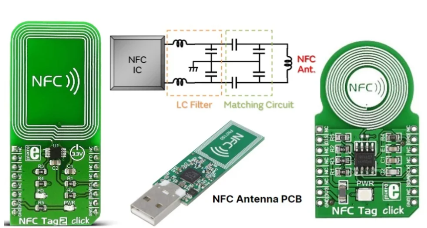
- RFID tags (chipless and UHF designs).
6. Future Trends
- Integration with metamaterials for enhanced performance.
- 3D-printed PCB antennas for customized shapes.
- AI-driven antenna design optimization.
- Energy-harvesting antennas for self-powered devices.
7. Conclusion
PCB-based small antennas provide an effective solution for modern wireless systems, balancing size, cost, and performance. By leveraging advanced miniaturization techniques, substrate engineering, and optimization algorithms, designers can overcome the inherent limitations of small antennas. Future advancements in materials and fabrication technologies will further expand their applications in next-generation communication systems.