Detailed description of the basic rules of PCB layout and wiring
PCB is also known as Printed Circuit Board. It can realize the line connection and function realization between electronic components, and is also an important component in power circuit design. Today, this article will introduce the basic rules of PCB layout and wiring.
1.Basic rules for component layout
- Layout according to circuit modules. Related circuits that realize the same function are called a module. Components in circuit modules should be concentrated nearby, and digital circuits and analog circuits should be separated;
- Components and devices shall not be mounted within 1.27mm around non-mounting holes such as positioning holes and standard holes, and components shall not be mounted within 3.5mm (for M2.5) and 4mm (for M3) around mounting holes such as screws;
- Avoid placing vias below components such as horizontally mounted resistors, inductors (plug-ins), and electrolytic capacitors to prevent vias from short-circuiting with component shells after wave soldering;
- The distance between the outer side of the component and the edge of the board is 5mm;
- The distance between the outer side of the mounted component pad and the outer side of the adjacent plug-in component is greater than 2mm;
- Metal shell components and metal parts (shielding boxes, etc.) cannot touch other components, cannot be close to printed lines and pads, and the spacing between them should be greater than 2mm. The outer dimensions of the positioning holes, fastener installation holes, elliptical holes and other square holes in the board should be greater than 3mm from the board edge;
- Heating elements cannot be close to wires and thermistors; high-heat devices should be evenly distributed;
- Power sockets should be arranged around the printed circuit board as much as possible, and the busbar terminals connected to the power sockets should be arranged on the same side. Special attention should be paid to not arranging power sockets and other welding connectors between connectors, so as to facilitate the welding of these sockets and connectors and the design and binding of power cables. The layout spacing of power sockets and welding connectors should be convenient for plugging and unplugging power plugs;
- Arrangement of other components:
All IC components are aligned on one side, and the polarity of polar components is clearly marked. The polarity marking on the same printed board shall not exceed two directions. When two directions appear, the two directions are perpendicular to each other;
- The board wiring should be properly dense. When the density difference is too large, it should be filled with mesh copper foil, and the grid should be greater than 8mil (or 0.2mm);
- There should be no through holes on the patch pads to prevent solder paste from leaking and causing component cold soldering. Important signal lines are not allowed to pass through the socket pins;
- The patch is aligned on one side, the character direction is consistent, and the package direction is consistent;
- The polarity marking direction of polarized devices on the same board should be kept consistent as much as possible

2.Component wiring rules
1.It is forbidden to lay wiring in the area within 1mm of the PCB board edge and within 1mm around the mounting hole;
2.The power line should be as wide as possible, not less than 18mil; the signal line width should not be less than 12mil; the CPU input and output lines should not be less than 10mil (or 8mil); the line spacing should not be less than 10mil;
3.Normal vias should not be less than 30mil;
4.Dual in-line: pad 60mil, aperture 40mil;
1/4W resistor: 51*55mil (0805 surface mount); pad 62mil, aperture 42mil when in-line;
Non-polar capacitor: 51*55mil (0805 surface mount); pad 50mil, aperture 28mil when in-line;
5.Note that the power line and ground line should be as radial as possible, and the signal line should not have loop routing.
How to improve anti-interference ability and electromagnetic compatibility?
When developing electronic products with processors, how to improve anti-interference ability and electromagnetic compatibility?
1.The following systems should pay special attention to anti-electromagnetic interference:
(1) Systems with extremely high microcontroller clock frequencies and extremely fast bus cycles.
(2) Systems containing high-power, high-current drive circuits, such as spark-generating relays, high-current switches, etc.
(3) Systems containing weak analog signal circuits and high-precision A/D conversion circuits.
2.To increase the system’s anti-electromagnetic interference ability, take the following measures:
(1) Select a low-frequency microcontroller:
Selecting a microcontroller with a low external clock frequency can effectively reduce noise and improve the system’s anti-interference ability. For square waves and sine waves of the same frequency, the high-frequency component in the square wave is much more than that in the sine wave. Although the amplitude of the high-frequency component of the square wave is smaller than that of the fundamental wave, the higher the frequency, the easier it is to emit and become a noise source. The most influential high-frequency noise generated by the microcontroller is about 3 times the clock frequency.
(2) Reduce distortion in signal transmission
Microcontrollers are mainly manufactured using high-speed CMOS technology. The static input current of the signal input end is about 1mA, the input capacitance is about 10PF, and the input impedance is quite high. The output end of the high-speed CMOS circuit has a considerable load capacity, that is, a considerable output value. If the output end of a gate is connected to the input end with a relatively high input impedance through a very long line, the reflection problem will be very serious, which will cause signal distortion and increase system noise. When Tpd>Tr, it becomes a transmission line problem, and signal reflection, impedance matching and other issues must be considered.
The delay time of the signal on the printed circuit board is related to the characteristic impedance of the lead, that is, it is related to the dielectric constant of the printed circuit board material. It can be roughly assumed that the transmission speed of the signal on the printed circuit board lead is about 1/3 to 1/2 of the speed of light. The Tr (standard delay time) of the commonly used logic telephone elements in the system composed of microcontrollers is between 3 and 18ns.
On a printed circuit board, the signal passes through a 7W resistor and a 25cm long lead, and the delay time on the line is roughly between 4 and 20ns. In other words, the shorter the signal lead on the printed circuit, the better, and the longest should not exceed 25cm. In addition, the number of vias should be as small as possible, preferably no more than 2.
When the rise time of the signal is faster than the signal delay time, it should be processed according to fast electronics. At this time, the impedance matching of the transmission line should be considered. For the signal transmission between integrated blocks on a printed circuit board, it is necessary to avoid the situation where Td>Trd. The larger the printed circuit board, the slower the system speed

The following conclusion summarizes a rule for printed circuit board design:
When the signal is transmitted on the printed circuit board, its delay time should not be greater than the nominal delay time of the device used.
(3) Reduce cross-interference between signal lines:
A step signal with a rise time of Tr at point A is transmitted to end B through lead AB. The delay time of the signal on line AB is Td. At point D, due to the forward transmission of the signal at point A, the reflection of the signal after reaching point B and the delay of line AB, a page pulse signal with a width of Tr will be induced after Td time. At point C, due to the transmission and reflection of the signal on line AB, a positive pulse signal with a width twice the delay time of the signal on line AB, that is, 2Td, will be induced. This is the cross-interference between signals. The strength of the interference signal is related to the di/at of the signal at point C and the distance between the lines. When the two signal lines are not very long, what is actually seen on AB is the superposition of two pulses.
Microcontrollers manufactured by CMOS technology have high input impedance, high noise, and high noise tolerance. Digital circuits can be superimposed with 100~200mv noise without affecting their operation. If the AB line in the figure is an analog signal, this interference becomes intolerable. If the printed circuit board is a four-layer board, one of which is a large area of ground, or a double-layer board, the reverse side of the signal line is a large area of ground, this cross-interference between signals will become smaller. The reason is that the large area of ground reduces the characteristic impedance of the signal line, and the reflection of the signal at the D end is greatly reduced. The characteristic impedance is inversely proportional to the square of the dielectric constant of the medium between the signal line and the ground, and is proportional to the natural logarithm of the thickness of the medium. If the AB line is an analog signal, to avoid the interference of the digital circuit signal line CD on AB, there should be a large area of ground under the AB line, and the distance from the AB line to the CD line should be greater than 2~3 times the distance between the AB line and the ground. Local shielding ground can be used, and ground wires can be laid on both sides of the lead with a lead.
(4) Reduce the noise from the power supply
While the power supply provides energy to the system, it also adds its noise to the power supply it supplies. The reset line, interrupt line, and other control lines of the microcontroller in the circuit are most susceptible to interference from external noise. Strong interference on the power grid enters the circuit through the power supply. Even in a battery-powered system, the battery itself has high-frequency noise. The analog signal in the analog circuit is even more vulnerable to interference from the power supply.
(5) Pay attention to the high-frequency characteristics of printed circuit boards and components
In high-frequency conditions, the distributed inductance and capacitance of leads, vias, resistors, capacitors, and connectors on printed circuit boards cannot be ignored. The distributed inductance of capacitors cannot be ignored, and the distributed capacitance of inductors cannot be ignored. Resistors produce reflections of high-frequency signals, and the distributed capacitance of leads will play a role. When the length is greater than 1/20 of the wavelength corresponding to the noise frequency, an antenna effect is generated, and the noise is emitted outward through the leads.
The vias on printed circuit boards cause about 0.6pf of capacitance.
The packaging material of an integrated circuit itself introduces 2~6pf of capacitance.
A connector on a circuit board has a distributed inductance of 520nH. A dual-row in-line 24-pin integrated circuit socket introduces a distributed inductance of 4~18nH.
These small distributed parameters can be ignored for microcontroller systems at lower frequencies; but special attention must be paid to high-speed systems.
(6) Components should be arranged in reasonable areas
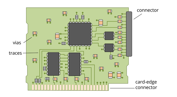
The arrangement of components on the printed circuit board should fully consider the problem of electromagnetic interference. One of the principles is that the leads between components should be as short as possible. In terms of layout, the analog signal part, high-speed digital circuit part, and noise source part (such as relays, high-current switches, etc.) should be reasonably separated to minimize the signal coupling between them.
G. Handle the ground wire well
On the printed circuit board, the power line and the ground line are the most important. The most important means to overcome electromagnetic interference is grounding.
For double-sided boards, the ground line layout is particularly particular. By adopting the single-point grounding method, the power supply and ground are connected to the printed circuit board from both ends of the power supply, one contact for the power supply and one contact for the ground. On the printed circuit board, there should be multiple return ground lines, which will converge to the point where the power supply is returned, which is the so-called single-point grounding. The so-called separation of analog ground, digital ground, and high-power device ground means that the wiring is separated and finally converges to this ground point. When connecting to signals outside the printed circuit board, shielded cables are usually used. For high-frequency and digital signals, both ends of the shielded cable should be grounded. For shielded cables used for low-frequency analog signals, one end should preferably be grounded.
Circuits that are very sensitive to noise and interference or circuits with particularly severe high-frequency noise should be shielded with metal covers.
(7) Use decoupling capacitors well.
Good high-frequency decoupling capacitors can remove high-frequency components up to 1GHZ. Ceramic chip capacitors or multilayer ceramic capacitors have better high-frequency characteristics. When designing a printed circuit board, a decoupling capacitor should be added between the power supply and ground of each integrated circuit. The decoupling capacitor has two functions: on the one hand, it is the energy storage capacitor of the integrated circuit, providing and absorbing the charging and discharging energy of the integrated circuit when it opens and closes; on the other hand, it bypasses the high-frequency noise of the device. The typical decoupling capacitor in a digital circuit is a 0.1uf decoupling capacitor with a distributed inductance of 5nH. Its parallel resonance frequency is about 7MHz, which means that it has a good decoupling effect on noise below 10MHz and has almost no effect on noise above 40MHz.
1uf, 10uf capacitors, parallel resonance frequency above 20MHz, are better for removing high-frequency noise. It is often beneficial to place a 1uf or 10uf high-frequency capacitor where the power supply enters the printed circuit board. Even battery-powered systems need this capacitor.
For every 10 or so integrated circuits, add a charging and discharging capacitor, or storage capacitor. The capacitance can be 10uf. It is best not to use electrolytic capacitors. Electrolytic capacitors are two layers of thin film rolled up. This rolled-up structure behaves as an inductor at high frequencies. It is best to use bile capacitors or polycarbonate capacitors.
The selection of decoupling capacitor value is not strict. It can be calculated according to C=1/f; that is, 0.1uf is used for 10MHz. For systems composed of microcontrollers, 0.1~0.01uf can be used.
3.Some experience in reducing noise and electromagnetic interference.
(1) If a low-speed chip can be used, do not use a high-speed one. High-speed chips are used in key places.
(2) A resistor can be used in series to reduce the jump rate of the upper and lower edges of the control circuit.
(3) Try to provide some form of damping for relays, etc.
(4) Use the lowest frequency clock that meets the system requirements.
(5) The clock generator should be as close as possible to the device that uses the clock. The quartz crystal oscillator housing should be grounded.
(6) Use a ground wire to circle the clock area and keep the clock line as short as possible.
(7) The I/O drive circuit should be as close as possible to the edge of the printed circuit board to allow it to leave the printed circuit board as soon as possible. The signals entering the printed circuit board should be filtered, and the signals coming from the high noise area should also be filtered. At the same time, use the method of series terminal resistance to reduce signal reflection.
(8) The unused end of the MCD should be connected to a high level, or to the ground, or defined as an output end. The ends of the integrated circuit that should be connected to the power ground should be connected and not left floating.
(9) The input ends of unused gate circuits should not be left floating. The positive input ends of unused op amps should be grounded and the negative input ends should be connected to the output ends.
(10) Try to use 45-degree fold lines instead of 90-degree fold lines for printed circuit boards to reduce the emission and coupling of high-frequency signals.
(11) The printed circuit boards are divided according to frequency and current switching characteristics. Noise components and non-noise components should be farther apart.
(12) Single-sided and double-sided boards use single-point power supply and single-point grounding. The power line and ground line should be as thick as possible. If the economy can afford it, use multi-layer boards to reduce the capacitance and inductance of the power supply and ground.
(13) Clock, bus, and chip select signals should be kept away from I/O lines and connectors.
(14) Analog voltage input lines and reference voltage terminals should be kept away from digital circuit signal lines, especially clocks.
(15) For A/D devices, it is better to unify the digital and analog parts rather than cross them.
(16) The clock line perpendicular to the I/O line has less interference than the parallel I/O line. The clock component pins should be kept away from the I/O cable.
(17) Keep component pins as short as possible, and keep decoupling capacitor pins as short as possible.
(18) Keep key lines as thick as possible, and add protective ground on both sides. High-speed lines should be short and straight.
(19) Do not run noise-sensitive lines parallel to high-current and high-speed switching lines.
(20) Do not run lines under quartz crystals or noise-sensitive devices.
(21) Do not form current loops around weak signal circuits and low-frequency circuits.
(22) Do not form a loop for any signal. If it is unavoidable, make the loop area as small as possible.
(23) Use a decoupling capacitor for each integrated circuit. Add a small high-frequency bypass capacitor next to each electrolytic capacitor.
(24) Use large-capacity tantalum capacitors or polycool capacitors instead of electrolytic capacitors as circuit charging and discharging energy storage capacitors. When using tubular capacitors, the casing must be grounded.

