Detailed explanation the difference between pcb single layer and double layers
In electronic product design ,pcb is the essential part .According to the numberof layers ,pcb can be divded into single-layer board and double-layer board.For many electronic engineers ,It is the basic that understanding the difference between single layer board and double layers board.This article will detail explain the difference between single layer board and double layers board and help you to make the best choice.
The definition of single layer board and double layers board
single-layer board:singe layer board is the basic type of pcb. It only has one side which is the conductive layers (copper foil),the other side is the Non-conductive materials.This design is simple,usually used in low -complex circuits like simple home appliances and electronic toys .
double-layer board :There are conductive layers in the pcb both sides,which means it can be true that electric connection by both side .Compare with the single layer board,double -layer board have the more complex circuits design that fit for the high demands electronic products like automotive electronics and consumer electronics,etc.
The main difference between single layer board and double layers board
1.layers number and density :single layer board only has the covered copper foil on one side,all of the component and electronic connection are concentrated on this side.double layer board has two layers copper foil .through via can achieved both side electronic connection. components can be put on both side to increase the component density .
2.Signal integrity :the distance between signal plane and ground plane in the single layer board is long.which may lead to higher signal loop path impedance and affect signal integrity.The lack of inner layers for the layout of power and ground planes in double-layer boards may cause signal integrity problems.
3. Application areas: Due to their simple design, single-layer boards are usually used for products that do not require complex circuits, such as simple home appliances and electronic toys. Double-layer boards are widely used in electronic devices that require higher functions, such as smart home devices, computer hardware, medical equipment, etc., because they can achieve more complex circuit designs.
4. Cost differences: The production process of single-layer boards is relatively simple and the cost is low. Since double-layer boards need to design circuits on both sides and connect through vias, their production process is more complicated and the cost is relatively high. Jiali Chuang PCB provides customers with cost-effective double-layer and multi-layer board solutions by optimizing the production process.
5.Electrical performance: Double-layer boards have better electrical performance in complex circuits because they have double-sided conductive layers, which can reduce signal interference and electromagnetic interference (EMI) during design. Single-layer boards are relatively weak in electrical performance due to being limited to one side, and are not suitable for applications with high-frequency signal transmission.
6.Flexibility: Although single-layer boards are simple in design, it is difficult to achieve diversified product designs. Double-layer boards are limited by impedance control and weak power distribution, and are not as flexible as multi-layer PCBs, and are limited by wiring space.
7. Miniaturization: Single-layer boards are difficult to miniaturize, which is one of the main reasons for their elimination. Although double-layer boards can use SMT technology or small components to reduce the size of electronics, they still have disadvantages.
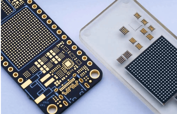
In addition to single-layer and double-layer boards, there is another type of PCB that is very important, that is, high-layer PCBs. High-layer has become one of the important trends in the future development of the PCB industry. Because with the further development of electronic information technology, the structure of electronic products is becoming more and more complex, and the functions are becoming more and more comprehensive, which has prompted PCB to develop towards highly integrated and miniaturized design, and the number of PCB layers is gradually increasing.
From personal computers, TVs to industrial machines, low-end servers and communication equipment, to high-end servers, high-end routers, communication base stations and supercomputers, high-layer PCBs are not only widely used, but also play an important role in them.
Because high-layer PCBs have extremely high requirements for process and technology, and their production is also very difficult, only a few companies have the ability to produce high-layer PCBs.


