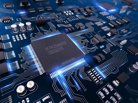
Detailed IC chip EMI design impact
Electromagnetic compatibility design often uses various control techniques. In general, the closer to the EMI source, the lower the cost of implementing EM control. Integrated circuit chips on PCBs are the primary source of energy for EMI, thereby simplifying EMI control in PCBs and system-level designs with a deep understanding of the internal features of integrated circuit chips.
When considering EMI control, design engineers and PCB board level design engineers should first consider the choice of IC chip.
Some features of integrated circuits such as package type, bias voltage and chip: technology (eg CMoS, ECI) and so on have a great impact on electromagnetic interference. The following will focus on the impact of IC on EMI control.
IC EMl source
IC EMI sources in the PCB are: digital integrated circuits from logic high to low logic conversion or logic low to high logic conversion process, the output of the square wave signal frequency caused by the EMl signal voltage and signal Current electric field and magnetic field chip capacitance and inductance.
The square wave generated at the output of the IC chip contains a wide range of sinusoidal harmonic components that make up the EMI frequency component of concern to engineers.

The highest EMI frequency, also known as the EMI emission bandwidth, is a function of the signal rise time, not the signal frequency.
The formula for calculating the EMI emission bandwidth is: f = 0.35 / Tr where the plant is the frequency in GHz and 7r is the signal rise time or fall time in ns.
It can be seen from the above formula that if the switching frequency of the circuit is 50MHz and the rising time of the integrated circuit chip used is 1ns, the maximum EMI emission frequency of the circuit will reach 350MHz, which is much larger than the switching frequency of the circuit. If the sink – rise time is 5 ribs Fs, then the maximum EMI emission frequency of the circuit will be as high as 700MHz.
Each voltage value in the circuit corresponds to a certain current, and the same voltage exists in each current.
When the IC’s output changes from logic high to logic low or logic low to logic high, these signal voltages and signal currents create electric and magnetic fields, and the highest frequencies of these electric and magnetic fields are the transmission bandwidth. The strength of electric and magnetic fields and the percentage of external radiation are not only a function of signal rise time but also depend on the control of the capacitance and inductance of the signal path between the signal source and the load point.
Therefore, the signal source is located on the PCB Of the sink, while the load is located inside other ICs, which may or may not be on the PCB.
In order to effectively control the EMI, not only need to focus on the exchange; Pat’s own capacitance and inductance, also need to pay attention to the presence of capacitors and inductors on the PCB.
When the signal voltage and the signal circuit between the pan is not close, the circuit capacitance will be reduced, so the inhibition of the electric field will be weakened, so that EMI increases; current in the circuit also exist the same situation, if Current is not the same as the return path; good, it is bound to increase the inductance of the loop, thereby enhancing the magnetic field, eventually leading to increased EMI. This fully shows that poor control of the electric field usually results in poor suppression of the magnetic field. The measures used to control the electromagnetic field in the circuit board are generally similar to those used to suppress the electromagnetic field in the IC package. Just as with PCB design, IC package design will greatly affect EMI.
A considerable part of the electromagnetic radiation in the circuit is caused by voltage transients in the power bus.
When the output of the sink send: jump and drive the connected PCB line is logic “high”, the sink chip will absorb current from the power supply to provide the output stage on the required energy. For the continuous conversion of the IC produced by ultra-high frequency current, the power bus on the PCB on the roller network to stop the sink output level. If the output stage has a signal rise time of 1.0ns, the IC should sink enough current from the power supply to drive the transmission line on the PCB in a short period of 1.0ns.
The voltage transient on the power bus depends on the path of the j-line of the power supply. Sense, to absorb the current and the current transmission time. The voltage transients are defined by the formula, L is the value of the inductance on the current path, dj is the change in current over the signal rise time interval, and dz is the change in the d stream transmission time (signal rise time).
Because the IC pins and internal circuitry are part of the power bus and the time taken to sink current and output signals also depends somewhat on the process technology of the sink, choosing the right sink can be largely controlled The three elements mentioned in the above formula.
Packaging Features in Electromagnetic Interference Control
IC packages usually include silicon-based chips, a small internal PCB and pads. Silicon-based chip is mounted on a small 64PCB, through the bonding wire to achieve the connection between the silicon-based chip and the pad, in some packages can also be connected directly to a small PCB to achieve silicon-based chip signal and power supply and sink package The connection between the corresponding pins, so that it realizes the external extension of the signal and power node on the silicon-based chip.
Therefore, the sink’s power and signal paths include stuffing chips, connections to small PCBs, PCB traces, and sink and package input and output pins. The control of capacitance and inductance (corresponding to electric and magnetic fields) depends very much on the design of the entire transmission path. Some of the design features will directly affect the capacitance and inductance of the entire IC chip package.
Look at the connection between the silicon-based chip and the internal small circuit board.
Many sink chips use bonding wires to make the connection between the neck silicon chip and an internal small circuit board, which is a very thin 6t wire between a silicon-based chip and an internal small circuit board. This technique is widely used because of the similar coefficient of thermal expansion (CU) between a silicon-based chip and an internal small circuit board. The chip itself is a silicon-based device with a thermal expansion coefficient that is comparable to typical PCB materials such as epoxy, The thermal expansion coefficient has a big difference. Such as: fruit silicon chip electrical connection points directly on the internal small PCB, then after a relatively short period of time, IC package internal temperature changes cause thermal expansion and contraction, this way the connection will be broken And failure. Bonding line is a way to adapt to this special environment lead, it can withstand greater bending deformation and not easily broken.
The problem with using bonding wires is that an increase in the current loop area per signal or power supply lead to an increase in inductance.
An excellent design that achieves lower inductance is the direct connection between the silicon-based chip and the internal PCB, which means the connection point of the silicon-based chip is directly bonded to the PCB’s land. This requires the choice of using a special PCB board-based material, this material should have a very low coefficient of thermal expansion. Choosing such a material will result in an increase in the overall cost of the sink chip. Therefore, a chip using such a technology is not common, but as long as such an IC that directly connects the silicon chip to the carrier PCB exists and is feasible in the design scheme, Then the use of such IC device is a better choice.
In general, in a sink package design, reducing the inductance and increasing the capacitance between the signal and the corresponding loop or between the supply and ground are the primary considerations when choosing an integrated circuit chip.
For example, small-pitch surface-mount packages and large-pitch surface mount packages: Processes should be given preference over sink chips packaged with a small-pitch surface-mount process package, and both types of surface mount package The IC chips are better than the via lead type package. The BGA packaged sink chip has the lowest lead inductance compared to any of the popular package types. From a capacitive and inductive control point of view, small packages and finer spacing always represent better performance.
An important feature of lead structure design is pin assignment.
Since the size of the inductor and capacitor depends on the signal or between the power supply and the return path, consider a sufficient number of return paths.
The power pin and the ground pin should be distributed in pairs. Each power pin should have its corresponding ground pin adjacently distributed. In this pin structure, multiple power pins and ground pin pairs should be allocated. Both of these features will greatly reduce the loop inductance between the power supply and ground, helping to reduce voltage transients on the power bus, reducing EAdI. Due to customary reasons, many of the current exchange chips in the market do not completely follow the above design rules, but IC designers and manufacturers have a deep understanding of the advantages of this design method. Therefore, when a new IC chip is designed and released, IC manufacturers Concerned about the power connection.
Ideally, you need to assign an adjacent signal return pin (such as a ground pin) for each signal pin.
The actual situation is not the case, many IC manufacturers are using other compromise method. In the BGA package, an effective design approach is to set up a signal return pin at the center of each set of eight signal pins, in this pin arrangement, between each signal and the signal return path Only one foot away from the distance. For quad flat pack (QFP) or other gullw-pack type ICs, it is not practical to place a signal return path in the center of the pack, even if this is done every 4 to 6 pins to place a signal return pin. It should be noted that different sink technology may use different signal return voltage. Some ICs use ground pins (such as TIL devices) as the signal return path, while others use power pins (such as most ECI ‘devices) as the return path for signals. Some ICs also use power tubes Foot and ground pins (such as most CMoS devices) serve as the return path for the signal. Therefore, design engineers must be familiar with the design of the IC chip logic used in series to understand their work.
The proper distribution of power and ground pins in IC chips not only reduces EMI but also greatly improves the groundboltnce effect.
When a device driving a transmission line tries to pull the transmission line down to a logic low, the ground-bounce still maintains the transmission line above a logic-low closed-loop level. Reflections from the ground can cause the circuit to fail or malfunction.
Another important issue in IC packaging is the PCB design inside the chip. The internal PCB is usually the largest part of the IC package.
If the internal PCB design allows for tight control of the capacitors and inductors, it will greatly improve the system’s Overall EMI performance. If this is a two-layer PCB, at least one side of the PCB is required to be a continuous ground plane layer and the other side of the PCB is the wiring layer for power and signal. More ideal case is a four-layer PCB, the middle two layers are the power and ground plane layer, the outer two layers as the signal wiring layer. Because the PCBs inside the package are usually very thin, the four-layer board design leads to two high-capacitance, low-inductance wiring layers that are well-suited for power distribution and the input and output signals that need to be tightly controlled into and out of the package. The low impedance planar layer greatly reduces the voltage transients of the power bus and greatly improves the EMI performance. This controlled signal line not only helps reduce EMI but also plays an important role in ensuring the integrity of the incoming and outgoing signals.


