Determination of PCB Thickness and Key Parameters in Design and Manufacturing
Abstract
Printed Circuit Boards (PCBs) are fundamental components in modern electronics, serving as the backbone for electrical connections between components. One of the critical factors influencing PCB performance is its thickness, which affects mechanical stability, signal integrity, thermal management, and manufacturability. This article explores the key considerations in determining PCB thickness, including material selection, layer count, impedance control, thermal requirements, and mechanical constraints. Additionally, it discusses standard thickness options, manufacturing tolerances, and the impact of thickness on high-frequency and high-power applications. By understanding these parameters, engineers can optimize PCB designs for reliability, performance, and cost-effectiveness.
1. Introduction
PCBs are essential in electronic devices, ranging from consumer electronics to industrial and aerospace systems. The thickness of a PCB plays a crucial role in its functionality, influencing factors such as:
- Mechanical Strength – Thicker PCBs are more rigid and resistant to bending.
- Signal Integrity – Thinner dielectrics affect impedance and crosstalk in high-speed designs.
- Thermal Performance – Thicker copper layers improve heat dissipation.
- Manufacturing Feasibility – Thinner PCBs are more flexible but harder to handle during assembly.
This paper examines how PCB thickness is determined based on design requirements, material properties, and application-specific constraints.
2. Standard PCB Thickness Options
The most common PCB thicknesses are standardized to ensure compatibility with manufacturing processes and component footprints.
2.1 Single and Double-Layer PCBs
- Typical thickness: 1.6 mm (most widely used).
- Other options: 0.8 mm, 1.0 mm, 1.2 mm, 2.0 mm.
2.2 Multilayer PCBs (4+ Layers)
- Standard thickness: 1.6 mm (balanced between rigidity and weight).
- Thinner options: 0.4 mm to 1.0 mm (used in compact devices like smartphones).
- Thicker options: 2.4 mm to 3.2 mm (for high-power or high-reliability applications).
2.3 Flexible and Rigid-Flex PCBs
- Typical range: 0.1 mm to 0.3 mm (for flex circuits).
- Rigid sections may follow standard thicknesses (e.g., 1.0 mm to 1.6 mm).
3. Key Parameters Influencing PCB Thickness Selection
3.1 Layer Count and Stack-Up Configuration
- More layers require thicker PCBs to accommodate dielectric and copper layers.
- High-density interconnects (HDI) may use thinner dielectrics (< 0.1 mm per layer).
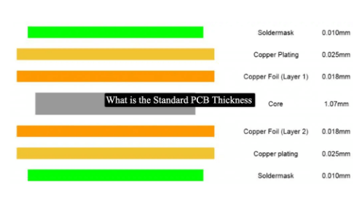
3.2 Dielectric Material (Substrate Choice)
- FR-4 (most common): Thickness depends on prepreg and core layers.
- High-frequency materials (Rogers, PTFE): Thinner dielectrics for controlled impedance.
- Metal-core PCBs: Thicker for thermal management (e.g., 1.0 mm to 3.0 mm).
3.3 Copper Weight and Thickness
- Standard copper thickness: 1 oz (35 µm), 2 oz (70 µm), or higher for power PCBs.
- Thicker copper increases overall PCB thickness due to plating and etching processes.
3.4 Impedance Control (High-Speed Design)
- Critical for RF and high-speed digital circuits (e.g., USB, HDMI, DDR).
- Thinner dielectrics (0.1 mm to 0.2 mm) help maintain consistent impedance.
3.5 Thermal and Mechanical Requirements
- Power electronics: Thicker PCBs (≥ 2.0 mm) for better heat dissipation.
- Vibration resistance: Thicker boards resist mechanical stress.
- Flex applications: Thin and flexible PCBs for wearable devices.
3.6 Manufacturing and Assembly Constraints
- Drilling aspect ratio: Thicker PCBs require larger drill holes (max 10:1 ratio).
- Solder mask application: Thinner PCBs may have coating challenges.
- Component compatibility: Some connectors and sockets require specific thicknesses.
4. Advanced Considerations in PCB Thickness Selection
4.1 High-Frequency and RF Applications
- Thin dielectrics reduce signal loss and parasitic capacitance.
- Materials like Rogers RO4003C offer tight thickness tolerances (±0.05 mm).
4.2 High-Power and High-Current Designs
- Thicker copper (≥ 3 oz) reduces resistive losses.
- Metal-core PCBs (e.g., Aluminum or Copper base) improve thermal conductivity.
4.3 Miniaturization and HDI PCBs
- Ultra-thin PCBs (0.2 mm to 0.4 mm) for wearables and IoT devices.
- Microvias and laser drilling enable thinner multilayer stacks.
5. Manufacturing Tolerances and Thickness Variations
- Standard tolerance: ±10% for overall thickness.
- Tight tolerance: ±5% or better for impedance-critical designs.
- Warpage risks increase with asymmetric layer stacks.
6. Conclusion
Selecting the appropriate PCB thickness involves balancing electrical performance, mechanical durability, thermal management, and manufacturability. Engineers must consider layer count, material properties, impedance requirements, and application-specific needs. By carefully evaluating these parameters, optimal PCB designs can be achieved for various industries, from consumer electronics to aerospace systems.
Future trends may push for thinner, high-performance PCBs with advanced materials, further emphasizing the importance of precise thickness control in PCB manufacturing.