Difference between hdi and hdr PCB
Understanding The Basics: HDI Vs. HDR PCB
In the realm of printed circuit boards (PCBs), technological advancements have led to the development of various types of PCBs to meet the growing demands of modern electronics. Among these, High-Density Interconnect (HDI) and High Dynamic Range (HDR) PCBs have emerged as significant innovations, each serving distinct purposes and applications. Understanding the differences between HDI and HDR PCBs is crucial for professionals in the electronics industry, as it enables them to make informed decisions when selecting the appropriate technology for their specific needs.
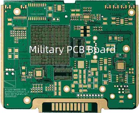
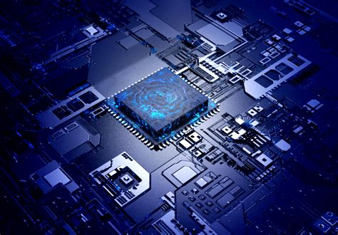
To begin with, HDI PCBs are characterized by their high-density attributes, which allow for more components to be placed on a smaller board.
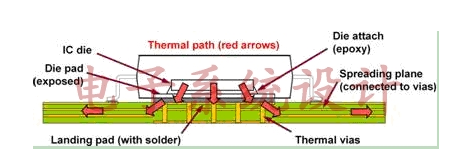
This is achieved through the use of microvias, blind vias, and buried vias, which facilitate the interconnection of multiple layers within the PCB. The primary advantage of HDI technology is its ability to support complex circuitry in compact designs, making it ideal for applications where space is at a premium, such as in smartphones, tablets, and other portable electronic devices. Furthermore, HDI PCBs offer improved electrical performance due to shorter signal paths, which reduce signal loss and enhance overall device efficiency.
In contrast, HDR PCBs are designed to support high dynamic range applications, which are essential in fields such as audio and video processing.
HDR technology focuses on delivering a wider range of luminance levels, providing more detail in both the darkest and brightest parts of an image or sound. This is particularly important in applications like high-definition televisions, cameras, and audio equipment, where the quality of output is paramount. HDR PCBs are engineered to handle the increased data processing requirements associated with high dynamic range signals, ensuring that the final output is both accurate and of superior quality.
While both HDI and HDR PCBs are integral to modern electronics, their differences lie in their core functionalities and applications.
HDI PCBs are primarily concerned with maximizing space efficiency and enhancing electrical performance in compact devices. On the other hand, HDR PCBs are focused on optimizing the quality of audio and visual outputs by managing high dynamic range signals effectively. This distinction is crucial for engineers and designers who must choose the appropriate PCB technology based on the specific requirements of their projects.
Moreover, the manufacturing processes for HDI and HDR PCBs also differ significantly.
HDI PCBs require advanced fabrication techniques to accommodate the intricate designs and high-density interconnections. This often involves laser drilling for microvias and precise layer alignment to ensure optimal performance. Conversely, HDR PCBs necessitate a focus on signal integrity and data processing capabilities, which may involve specialized materials and design considerations to handle the high bandwidth and dynamic range demands.
In conclusion, while HDI and HDR PCBs both represent significant advancements in PCB technology, they cater to different needs within the electronics industry.
HDI PCBs excel in applications where space and electrical performance are critical, whereas HDR PCBs are indispensable in scenarios where high-quality audio and visual outputs are required. Understanding these differences is essential for professionals tasked with selecting the right PCB technology, as it ensures that the chosen solution aligns with the specific demands of their application, ultimately leading to more efficient and effective electronic devices.
Key Design Differences Between HDI And HDR PCBs
In the realm of printed circuit board (PCB) design, understanding the nuances between different types of PCBs is crucial for engineers and designers. Two prominent types that often come into discussion are High-Density Interconnect (HDI) PCBs and High-Density Rigid (HDR) PCBs. While both serve the purpose of accommodating complex electronic circuits, they differ significantly in their design and application, which can influence the choice of one over the other depending on the specific requirements of a project.
To begin with, HDI PCBs are characterized by their ability to incorporate a higher number of interconnections in a smaller area.
This is achieved through the use of microvias, blind vias, and buried vias, which allow for more layers and finer lines and spaces. Consequently, HDI PCBs are ideal for applications where space is at a premium, such as in smartphones, tablets, and other compact electronic devices. The design of HDI PCBs often involves advanced techniques like sequential lamination and laser drilling, which enable the creation of intricate circuit patterns that are not feasible with traditional PCBs.
In contrast, HDR PCBs, while also designed to handle high-density circuits, are primarily focused on maintaining rigidity and structural integrity.
These PCBs are typically used in applications where mechanical stability is paramount, such as in automotive and industrial electronics. HDR PCBs are constructed using rigid materials that provide durability and resistance to environmental stressors. This makes them suitable for environments where the PCB might be subjected to physical shocks or extreme temperatures. The design of HDR PCBs often involves thicker substrates and robust materials, which contribute to their strength and reliability.
Transitioning from the structural aspects, another key difference lies in the manufacturing processes of HDI and HDR PCBs.
The production of HDI PCBs is more complex and requires precision equipment to handle the fine features and multiple layers. This complexity often results in higher production costs and longer lead times. However, the benefits of miniaturization and enhanced performance often justify these costs in high-tech applications. On the other hand, HDR PCBs, while still requiring careful manufacturing processes, do not typically involve the same level of intricacy as HDI PCBs. This can lead to more cost-effective production, especially for applications where the primary concern is durability rather than miniaturization.
Furthermore, the choice between HDI and HDR PCBs can also be influenced by the specific electrical performance requirements of a project.
HDI PCBs, with their ability to support high-speed signals and reduce signal loss, are often preferred in applications that demand high-frequency performance. This is particularly relevant in telecommunications and computing, where efficient signal transmission is critical. Conversely, HDR PCBs, with their robust construction, are better suited for applications where electrical performance is secondary to physical resilience.
In conclusion, while both HDI and HDR PCBs are designed to support high-density circuits, their key design differences lie in their focus on miniaturization versus structural integrity. The decision to use one over the other should be guided by the specific needs of the application, considering factors such as space constraints, environmental conditions, manufacturing costs, and electrical performance requirements. Understanding these differences is essential for making informed decisions in PCB design and ensuring the success of electronic projects.
Applications And Use Cases: HDI And HDR PCBs
High-Density Interconnect (HDI) and High Dynamic Range (HDR) printed circuit boards (PCBs) are two distinct technologies that serve different purposes in the electronics industry. Understanding their applications and use cases is crucial for professionals seeking to optimize their designs and enhance the performance of electronic devices. While both HDI and HDR PCBs are pivotal in advancing technology, they cater to different needs and industries.
HDI PCBs are primarily used in applications where space and weight are critical constraints.
These boards are characterized by their higher wiring density per unit area, which is achieved through the use of finer lines and spaces, smaller vias, and capture pads. This allows for more components to be placed on both sides of the board, making them ideal for compact and lightweight devices. Consequently, HDI PCBs are extensively used in the production of smartphones, tablets, and other portable electronic devices. The miniaturization of components without compromising performance is a significant advantage of HDI technology, enabling manufacturers to create sleek, high-performance gadgets that meet consumer demands for portability and functionality.
In addition to consumer electronics, HDI PCBs find applications in the automotive industry, where they are used in advanced driver-assistance systems (ADAS) and infotainment systems.
The ability to integrate multiple functions into a single board while maintaining reliability and performance is crucial in automotive applications, where space is often limited, and safety is paramount. Furthermore, HDI technology is employed in the aerospace and defense sectors, where the need for lightweight and compact systems is even more pronounced. The high reliability and performance of HDI PCBs make them suitable for mission-critical applications, such as avionics and military communication systems.
On the other hand, HDR PCBs are designed to support high dynamic range imaging and display technologies.
HDR technology enhances the contrast and color range of displays, providing a more realistic and immersive viewing experience. This is achieved by increasing the range of luminance levels that a display can produce, from the darkest blacks to the brightest whites. HDR PCBs are integral to the functioning of HDR displays, as they manage the complex signal processing required to produce high-quality images.
The primary application of HDR PCBs is in the consumer electronics industry, particularly in televisions, monitors, and smartphones that support HDR content.
As consumers increasingly demand better picture quality, manufacturers are incorporating HDR technology into their products to meet these expectations. Beyond consumer electronics, HDR PCBs are also used in professional video production and broadcasting equipment, where accurate color representation and contrast are essential for producing high-quality content.
In summary, while HDI and HDR PCBs serve different purposes, both are essential in advancing modern technology. HDI PCBs are crucial for miniaturization and integration in compact devices, making them indispensable in industries such as consumer electronics, automotive, aerospace, and defense. Meanwhile, HDR PCBs play a vital role in enhancing visual experiences, primarily in the realm of display technologies. Understanding the distinct applications and use cases of these technologies allows engineers and designers to make informed decisions, ultimately leading to the development of innovative and high-performing electronic devices.
Manufacturing Challenges: HDI Compared To HDR PCBs
In the realm of printed circuit board (PCB) manufacturing, the advent of advanced technologies has led to the development of various types of PCBs, each designed to meet specific requirements. Among these, High-Density Interconnect (HDI) and High-Density Rigid (HDR) PCBs have emerged as prominent solutions, each offering unique advantages and challenges. Understanding the manufacturing challenges associated with HDI and HDR PCBs is crucial for industry professionals seeking to optimize production processes and ensure product reliability.
To begin with, HDI PCBs are characterized by their ability to accommodate a higher density of components on a smaller board area.
This is achieved through the use of microvias, blind and buried vias, and finer trace widths and spaces. The primary challenge in manufacturing HDI PCBs lies in the precision required for drilling and plating these microvias. As the size of vias decreases, the margin for error becomes significantly smaller, necessitating advanced equipment and meticulous process control. Moreover, the use of multiple lamination cycles in HDI PCB fabrication can introduce additional complexity, as each cycle must be carefully managed to prevent misalignment and ensure the integrity of the final product.
In contrast, HDR PCBs are designed to provide enhanced mechanical strength and thermal performance, making them suitable for applications that demand high reliability under challenging conditions.
The manufacturing challenges associated with HDR PCBs primarily revolve around the materials used and the processes required to achieve the desired rigidity and thermal properties. For instance, selecting the appropriate substrate material is critical, as it must offer both the necessary mechanical support and thermal conductivity. Additionally, the lamination process for HDR PCBs often involves higher temperatures and pressures, which can introduce potential issues such as delamination or warping if not properly controlled.
Despite these distinct challenges, there are commonalities in the manufacturing processes of HDI and HDR PCBs that warrant consideration.
Both types of PCBs require precise etching techniques to define the intricate circuit patterns, and any deviation from the intended design can lead to functional failures. Furthermore, the soldering process for both HDI and HDR PCBs must be carefully managed to prevent defects such as solder bridging or insufficient solder joints, which can compromise the electrical performance of the board.
Transitioning from the technical aspects to the broader implications, it is evident that the manufacturing challenges associated with HDI and HDR PCBs have significant implications for the electronics industry.
As devices continue to shrink in size while increasing in functionality, the demand for high-performance PCBs is expected to grow. Consequently, manufacturers must invest in advanced technologies and skilled personnel to address the complexities of HDI and HDR PCB production. This includes adopting automated inspection systems to ensure quality control and implementing robust process management strategies to minimize defects and improve yield.
In conclusion, while HDI and HDR PCBs each present unique manufacturing challenges, they also offer significant opportunities for innovation and advancement in the electronics industry. By understanding and addressing these challenges, manufacturers can enhance their production capabilities and deliver high-quality products that meet the evolving demands of modern technology. As the industry continues to advance, the ability to effectively navigate the complexities of HDI and HDR PCB manufacturing will be a key determinant of success.