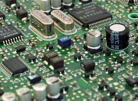
Differences and usages of Fill, Polygon Pour, and Plane in Altium
Fill means drawing a solid copper sheet, connecting all the connections and vias in the area together, regardless of whether they belong to the same network. If there are two networks, VCC and GND, in the drawn area, the Fill command will connect the elements of these two networks together, which may cause a short circuit.
Polygon Pour: pouring copper.
Its function is similar to Fill, and it also draws a large area of copper sheet; but the difference lies in the word “pour”. Pour copper has unique intelligence and will actively distinguish the networks of vias and solder joints in the copper pouring area. If the via and solder joint belong to the same network, pour copper will connect the via, solder joint and copper sheet together according to the set rules. Otherwise, the copper sheet will maintain a safe distance from the via and solder joint. The intelligence of pouring copper is also reflected in its ability to automatically delete dead copper.
Polygon Pour Cutout: Establish a copper cutting area in the copper pouring area. For example, some important networks or components need to be hollowed out at the bottom, such as common RF signals. There is also the RJ45 area under the transformer.
Polygon Pour: Cut the copper pouring area. For example, if the copper pouring needs to be optimized or reduced, Line can be used to split it into two copper pouring areas in the reduced area, and the unwanted copper pouring area can be directly deleted.
In summary, Fill will cause short circuits, so why use it?
Although Fill has its shortcomings, it also has its use environment. For example, when there are high-current power chips such as LM7805 and AMC2576, a large area of copper is required to dissipate heat for the chip. There can only be one network on this copper sheet, and the Fill command is just right.
Therefore, the Fill command is often used in the early stages of circuit board design. After the layout is completed, use Fill to draw all special areas to avoid mistakes in the subsequent design process.
In short, in the process of circuit board design, these two tools are used in conjunction with each other.
Plane: Plane layer (negative film), suitable for the whole board with only one power supply or ground network. If there are multiple power supplies or ground networks, you can use line to draw a closed box in a certain power supply or ground area, and then double-click the closed box to assign the corresponding power supply or ground network to this area. It can reduce a lot of engineering data compared to add layer (positive film layer), and the computer’s response speed is faster when processing high-speed PCB. The benefits of plane can be deeply experienced in the process of revision or modification.
Good method 1: When repairing copper, you can use PLANE [shortcut key P+Y] to repair obtuse angles.
Good method 2: Select the copper skin that needs to be repaired, and the shortcut key M+G can adjust the shape of the copper skin at will.