Different types of pcb manufacturing techniques
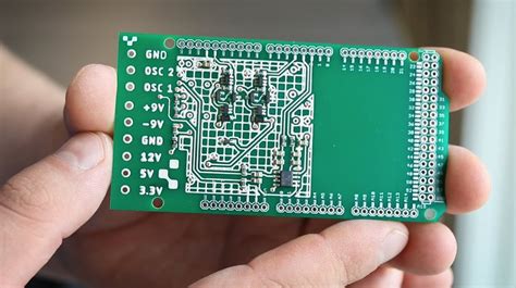
Surface Mount Technology (SMT) in PCB Manufacturing
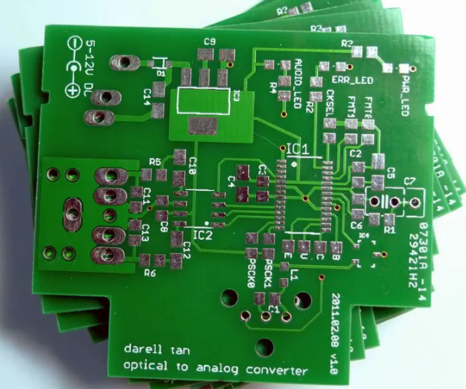
Surface Mount Technology (SMT) has revolutionized the field of printed circuit board (PCB) manufacturing, offering a more efficient and compact method of assembling electronic components. This technique involves mounting components directly onto the surface of the PCB, as opposed to the traditional through-hole method, which requires inserting component leads into drilled holes. SMT has become the preferred choice for many manufacturers due to its numerous advantages, including reduced size and weight of the final product, increased automation, and improved performance.
To begin with, one of the primary benefits of SMT is the ability to produce smaller and lighter electronic devices.
As consumer demand for compact and portable gadgets continues to rise, manufacturers are under pressure to minimize the size of their products. SMT addresses this need by allowing components to be placed on both sides of the PCB, thereby maximizing the use of available space. This results in a significant reduction in the overall footprint of the device, making it ideal for applications where space is at a premium.
Moreover, SMT facilitates a higher degree of automation in the manufacturing process.
Unlike through-hole technology, which often requires manual intervention to insert and solder components, SMT is highly compatible with automated assembly lines. This automation not only speeds up production but also enhances precision and consistency, leading to higher quality products. Automated machines can place thousands of components per hour with remarkable accuracy, reducing the likelihood of human error and ensuring that each PCB meets stringent quality standards.
In addition to size and automation benefits, SMT also contributes to improved electrical performance.
The shorter leads used in surface-mounted components result in lower inductance and resistance, which can enhance the overall performance of the circuit. This is particularly important in high-frequency applications where signal integrity is crucial. Furthermore, the reduced lead length minimizes the risk of parasitic capacitance, which can adversely affect circuit performance. As a result, SMT is often the preferred choice for high-speed and high-frequency electronic devices.
Despite these advantages, it is important to acknowledge that SMT is not without its challenges.
The smaller size of surface-mounted components can make them more difficult to handle and inspect, requiring specialized equipment and techniques. Additionally, the rework and repair of SMT assemblies can be more complex compared to through-hole assemblies, as the components are more densely packed and may require advanced skills to replace or repair. However, advancements in inspection technologies, such as automated optical inspection (AOI) and X-ray inspection, have mitigated some of these challenges by providing manufacturers with the tools needed to ensure quality and reliability.
In conclusion, Surface Mount Technology has become a cornerstone of modern PCB manufacturing, offering numerous benefits that align with the demands of today’s electronic industry.
Its ability to produce smaller, lighter, and more efficient devices, coupled with the advantages of automation and improved electrical performance, make it an attractive option for manufacturers. While there are challenges associated with SMT, ongoing advancements in technology continue to address these issues, further solidifying its position as a leading technique in PCB manufacturing. As the industry evolves, it is likely that SMT will continue to play a pivotal role in shaping the future of electronics.
Through-Hole Technology: A Traditional PCB Manufacturing Method
Through-hole technology (THT) has long been a cornerstone in the field of printed circuit board (PCB) manufacturing. This traditional method, which involves inserting component leads through pre-drilled holes on a PCB and soldering them to pads on the opposite side, has been instrumental in the development and evolution of electronic devices. Despite the advent of more advanced techniques, through-hole technology remains relevant due to its unique advantages and specific applications.
Initially, through-hole technology was the predominant method for mounting components on PCBs.
Its robustness and reliability made it the preferred choice for many applications, particularly those requiring high mechanical strength. Components mounted using THT are securely fastened to the board, making them less susceptible to damage from physical stress or environmental factors. This characteristic is especially beneficial in applications such as aerospace, automotive, and industrial equipment, where durability and reliability are paramount.
Moreover, through-hole technology facilitates easier manual assembly and inspection.
The larger size of through-hole components compared to their surface-mount counterparts allows for straightforward handling and placement, which is advantageous in prototyping and small-scale production. Additionally, the visibility of solder joints on the opposite side of the board simplifies the inspection process, enabling quick identification of potential issues.
However, as electronic devices have become increasingly compact and complex, the limitations of through-hole technology have become more apparent.
The need for miniaturization and higher component density has driven the industry towards surface-mount technology (SMT), which allows for smaller components and more efficient use of board space. Despite this shift, through-hole technology continues to hold its ground in specific niches where its benefits outweigh its drawbacks.
One of the primary challenges associated with through-hole technology is the requirement for drilling holes, which adds an extra step to the manufacturing process and increases production time and cost.
Additionally, the larger size of through-hole components limits the potential for miniaturization, making it less suitable for modern consumer electronics that demand compact designs. Nevertheless, in applications where space is not a critical constraint, the reliability and strength of through-hole connections remain highly valued.
Furthermore, through-hole technology is often used in conjunction with surface-mount technology in a hybrid approach.
This combination leverages the strengths of both methods, allowing manufacturers to optimize the design and functionality of PCBs. For instance, through-hole components may be used for connectors, transformers, or other parts that require strong mechanical bonds, while surface-mount components are employed for the majority of the circuitry to save space and reduce weight.
In conclusion, through-hole technology, despite being a traditional method, continues to play a vital role in PCB manufacturing.
Its enduring relevance is attributed to its robustness, ease of assembly, and suitability for specific applications where mechanical strength is crucial. While surface-mount technology has largely taken over in terms of miniaturization and efficiency, through-hole technology remains indispensable in certain sectors. As the electronics industry continues to evolve, the integration of both through-hole and surface-mount technologies will likely persist, ensuring that each method’s unique advantages are fully utilized in the creation of innovative and reliable electronic devices.
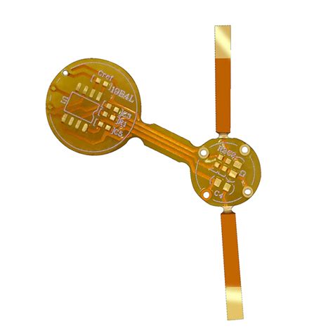
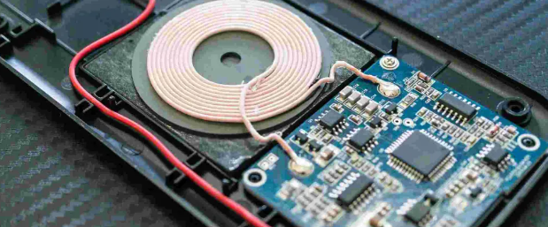
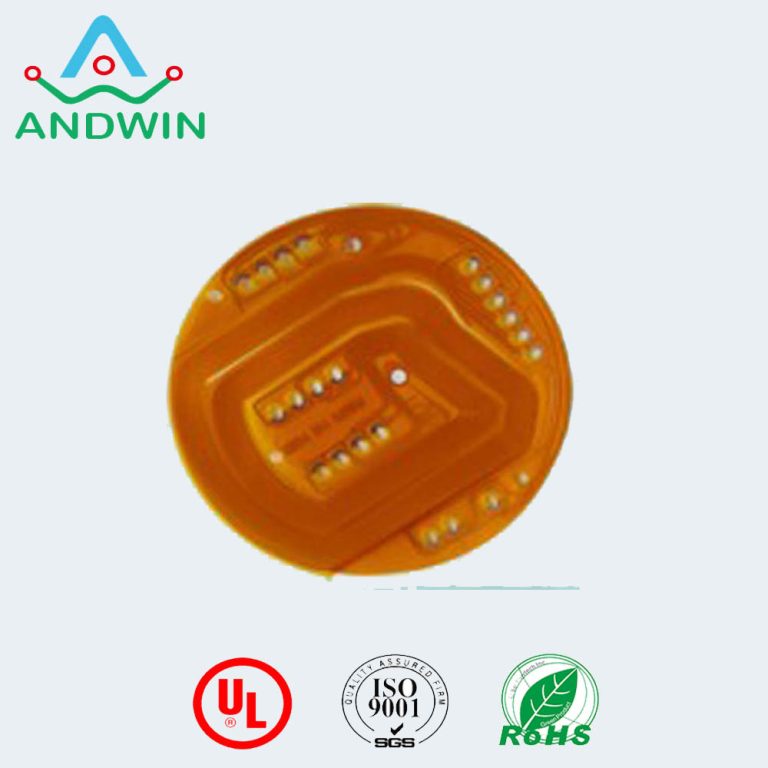
Flexible PCB Manufacturing: Techniques and Applications
Flexible printed circuit boards (PCBs) have become an integral component in modern electronics, offering a versatile solution for a wide range of applications. These PCBs are characterized by their ability to bend and flex, which allows them to be used in devices where space and weight are critical considerations. The manufacturing techniques for flexible PCBs are distinct from those used for rigid PCBs, and understanding these methods is essential for optimizing their performance and application.
One of the primary techniques used in flexible PCB manufacturing is the subtractive process.
This method involves starting with a copper-clad flexible substrate, typically made of polyimide, and selectively removing unwanted copper to create the desired circuit pattern. The subtractive process is often achieved through chemical etching, where a photoresist is applied to the substrate, exposed to ultraviolet light through a mask, and then developed to reveal the circuit pattern. The exposed copper is subsequently etched away, leaving behind the desired circuitry. This technique is favored for its precision and ability to produce fine line widths, making it suitable for high-density applications.
In addition to the subtractive process, the additive process is another technique employed in flexible PCB manufacturing.
Unlike the subtractive method, the additive process involves building up the circuit pattern by selectively depositing copper onto the substrate. This can be achieved through techniques such as electroless plating or direct printing. The additive process is advantageous in applications where material conservation is critical, as it minimizes waste by only depositing copper where needed. Furthermore, it allows for greater flexibility in design changes, as modifications can be made without the need to start from scratch.
Another important technique in flexible PCB manufacturing is the use of multilayer construction.
This involves stacking multiple layers of flexible circuits to create a single, cohesive unit. Multilayer flexible PCBs are particularly useful in complex applications where space is limited, as they allow for increased circuit density without expanding the footprint of the board. The layers are typically bonded together using adhesive materials, and vias are used to establish electrical connections between the layers. This technique requires precise alignment and lamination processes to ensure the integrity and functionality of the final product.
The applications of flexible PCBs are vast and varied, spanning industries such as consumer electronics, automotive, medical devices, and aerospace.
In consumer electronics, flexible PCBs are commonly found in smartphones, tablets, and wearable devices, where their lightweight and compact nature is highly valued. In the automotive industry, they are used in applications such as airbag systems and dashboard displays, where their ability to withstand harsh environments and vibrations is crucial. Medical devices benefit from flexible PCBs due to their biocompatibility and ability to conform to the human body, making them ideal for use in diagnostic and monitoring equipment. In aerospace, the lightweight and durable nature of flexible PCBs makes them suitable for use in satellites and other space-bound equipment.
In conclusion, the manufacturing techniques for flexible PCBs, including subtractive and additive processes, as well as multilayer construction, play a critical role in their performance and application. As technology continues to advance, the demand for flexible PCBs is expected to grow, driven by their unique properties and the increasing need for miniaturization and versatility in electronic devices. Understanding these manufacturing techniques is essential for engineers and designers looking to leverage the benefits of flexible PCBs in their projects.
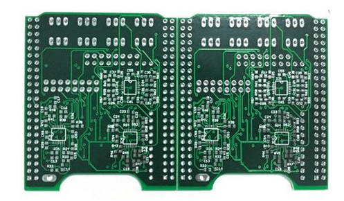
Advanced PCB Manufacturing: High-Density Interconnect (HDI) Techniques
In the realm of advanced electronics, the demand for compact, efficient, and high-performance devices has led to significant innovations in printed circuit board (PCB) manufacturing. Among these innovations, High-Density Interconnect (HDI) techniques have emerged as a pivotal advancement, enabling the production of PCBs with higher wiring density per unit area. This evolution is crucial for supporting the miniaturization of electronic components while maintaining or even enhancing their functionality. As we delve into the intricacies of HDI techniques, it becomes evident that these methods are not only transformative but also essential for the future of electronic design and manufacturing.
To begin with, HDI PCBs are characterized by their finer lines and spaces, smaller vias, and capture pads, as well as higher connection pad density.
These features are achieved through various advanced manufacturing techniques, each contributing uniquely to the overall performance and reliability of the final product. One of the primary techniques employed in HDI manufacturing is the use of microvias. Unlike traditional vias, microvias are significantly smaller and can be placed directly on top of each other, known as stacked vias, or staggered, known as staggered vias. This capability allows for more complex routing and greater component density, which is particularly beneficial in applications where space is at a premium.
Moreover, laser drilling is a critical process in the creation of microvias.
This technique offers precision and accuracy, enabling the production of extremely small vias that are essential for HDI PCBs. The use of laser technology ensures that the vias are clean and have smooth walls, which is vital for maintaining signal integrity and reducing the risk of defects. Additionally, laser drilling allows for greater flexibility in design, as it can accommodate various materials and thicknesses, further enhancing the versatility of HDI PCBs.
Another significant technique in HDI manufacturing is the use of sequential lamination.
This process involves the layering of multiple dielectric and conductive materials to create a multi-layered PCB. Sequential lamination allows for the integration of more complex circuitry within a smaller footprint, which is indispensable for modern electronic devices that require high functionality in a compact form. The ability to add layers incrementally also provides designers with the flexibility to modify and optimize the board layout as needed, ensuring that the final product meets the specific requirements of the application.
Furthermore, the incorporation of advanced materials plays a crucial role in HDI PCB manufacturing.
High-performance substrates, such as polyimide and liquid crystal polymer, offer superior thermal and electrical properties, which are essential for supporting the high-speed and high-frequency applications that HDI PCBs often serve. These materials not only enhance the performance of the PCB but also contribute to its durability and reliability, making them ideal for use in demanding environments.
In conclusion, the development and implementation of HDI techniques in PCB manufacturing represent a significant leap forward in the electronics industry. By enabling higher component density, improved performance, and greater design flexibility, these techniques are paving the way for the next generation of electronic devices. As technology continues to advance, the importance of HDI PCBs will only grow, underscoring the need for ongoing innovation and refinement in manufacturing processes. Through the continued exploration and adoption of these advanced techniques, manufacturers can meet the ever-evolving demands of the market, ensuring that they remain at the forefront of technological progress.