Digital-analog hybrid PCB design, knowing these will make you get twice the result with half the effort
1.Understanding the basic concepts of digital-analog hybrid design
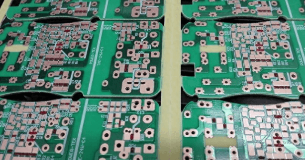
Many products include digital-analog hybrid PCB design, and different signals have different anti-interference capabilities. In the interconnection design process, the crosstalk between different signals must be reasonably controlled to ensure the index requirements of the final product.
It is very important to understand the following basic concepts. Mastering the basic concepts of digital-analog hybrid design will help understand the strict layout and wiring design rules formulated later, so that when designing the digital-analog hybrid of the terminal product, the important constraint rules will not be easily discounted. And it helps to flexibly and effectively deal with the crosstalk problems that may be encountered in digital-analog hybrid design.
2.The important difference between analog signals and digital signals in anti-interference ability
The digital signal level has a strong anti-interference ability, while the analog signal has a poor anti-interference ability.
For example, a digital signal with a 3V level can tolerate even if it receives a 0.3V crosstalk signal, and it will not affect the logic state. However, in the field of analog signals, some signals are extremely weak. For example, the receiving sensitivity of a GSM mobile phone can reach an index of -110dBm, which is only equivalent to the effective value of a sine wave of 0.7uV. Even if the in-band interference noise of the order of uV is received at the front end of the LNA, it is enough to significantly degrade the receiving sensitivity of the base station. This slight interference may come from the small noise on the digital control signal line or the power ground line.
From the perspective of the system, digital signals are generally only transmitted on the board or in the frame. For example, memory bus signals, power control signals, etc., as long as the interference received from the transmitter to the receiver is not enough to affect the judgment of the logical state. The analog signal needs to go through a series of processes such as modulation, frequency conversion, amplification, transmission, space propagation, reception, and demodulation before it can be restored. During this process, noise is constantly superimposed on the signal. From the perspective of the system, it is necessary to ensure that the final signal-to-noise ratio meets the requirements in order to demodulate correctly. The biggest interference comes from the attenuation and noise of space propagation. In order to achieve better communication performance, the crosstalk introduced by the interconnection within the board must be minimized as much as possible.
Therefore, it can be considered that the crosstalk requirements of analog signals are dozens of times higher than those of digital signals, and may even reach tens of thousands of times.
3.High-precision ADC and DAC circuits
Ideally, the relationship between the signal-to-noise ratio and the number of conversion bits of linear ADC and DAC circuits is:
For 14-bit linear ADC and DAC, if the least significant bit (LSB) is valid, the theoretical signal-to-noise ratio can be calculated to be 86dBc. Compared with the crosstalk requirement of about 20dBc for digital circuits, the noise requirements of high-precision 14-bit linear ADC and DAC are at least 1000 times higher than those of digital signals. Of course, if the least significant bit is only 11 bits, the crosstalk requirements can be appropriately lowered, but they are still much higher than those of digital signals.
The above two situations show that in the digital-analog hybrid board, the analog circuit is extremely susceptible to interference, which will affect indicators such as the signal-to-noise ratio. Therefore, in the PCB design process of the digital-analog hybrid board, high requirements must be placed on layout and wiring.
4.Digital signals are strong interference sources for analog signals
The level of digital signals is very high compared to analog signals, and digital signals contain rich harmonic frequencies. Therefore, digital signals are strong interference sources for analog signals. In particular, high-current clock signals, switching power supplies, etc. are strong interference sources that need to be paid attention to in digital-analog hybrid design.
5.The fundamental purpose of digital-analog hybrid interconnection design
We can understand the digital-analog design problem in this way. For digital circuits, we follow the design rules of digital circuits. In the digital circuit area, larger interference can be allowed to exist, as long as it does not affect the system function realization and external EMC indicators.
The “larger” we are talking about here is relative to analog circuits. For digital circuits, we do not need to and cannot control the existence of crosstalk like analog circuits. For analog circuits, we must follow the design rules of analog circuits. The interference allowed in the analog circuit area is much smaller than that in the digital circuit area.
The purpose of digital-analog hybrid interconnection design is to ensure that the interference of digital signals only exists in the digital signal area through reasonable layout, wiring, shielding, filtering, power supply and ground division and other design methods.
The contents we need to focus on include interference sources, sensitive circuits, and interference paths. The following will describe the layout and routing principles adopted from these three aspects. Successful digital-analog hybrid single-board design can only be achieved by paying careful attention to every step and every detail in the entire process, which means that thorough and careful planning must be carried out at the beginning of the design, and the progress of each design step must be comprehensively and continuously evaluated. The layout and routing must be carefully checked and verified to ensure that the layout and routing rules are 100% followed. Otherwise, an improper signal line routing will completely destroy an originally very good circuit board.
Rules are dead. Only by deeply understanding the principles through the rules can we ensure that we can correctly apply the rules and complete excellent designs.
6.Distinguishing between circuit types
Before explaining the layout rules of digital-analog hybrid design, we now distinguish between the interference sources, sensitive circuits, and interference paths on the terminal board. Understanding these interference sources and sensitive circuits can help us correctly formulate layout and routing plans. In addition, understanding the interference paths is crucial.
7.Analog circuits
For terminal products, analog circuits include all RF circuits, RF power supplies, RF control circuits, digital-to-analog conversion circuits, and audio circuits. All of the above analog circuits are sensitive circuits, and the sensitive circuits that need special attention include the frequency termination circuit (including the local oscillator signal, the power supply of the frequency synthesizer circuit, and the control signal), the receiving front-end circuit, and the audio circuit.
8.Interference sources
The interference sources include all digital circuits and high-power RF circuits (power amplifiers, antennas, and other high-power RF circuits). The interference sources that need special attention include clock circuits, switching power supplies, high-current power lines, power amplifier circuits, and antenna circuits. The interference of RF signals such as power amplifiers and antennas is analyzed in the RF design section of this specification.
9.Interference paths
For digital-analog hybrid design, the interference paths that need to be paid attention to include: space radiation, power ground (plane or trace), digital-to-analog conversion circuits, and various control signals of analog circuits.
(1) Space radiation: Circuits close to each other will generate crosstalk through radiation. This is the same as the concept of digital signal crosstalk, but it should be noted that the crosstalk that analog signals can tolerate is much smaller than that of digital signals. Therefore, it is necessary to control crosstalk during the layout stage. The way to reduce space radiation is generally to increase the layout distance and use a shielding box.
(2) Power ground: The power ground is a common loop for digital and analog circuits, so interference signals may be transmitted to sensitive circuits through the power ground conductor. The way to control power ground crosstalk is to use filter devices and power ground segmentation appropriately.
(3) Digital-to-analog conversion circuit: It is an interface between analog and digital signals. If the layout or wiring is not handled properly, such as unclear division of digital and analog circuit layout and interlaced routing, crosstalk may occur.
(4) Analog control signal: The ideal analog device should be that the control signal and analog circuit are isolated inside the device, and the control signal only needs to ensure the correct logic level. However, the device often cannot do this, and the interference signal on the control signal may be directly coupled to the analog circuit. The solution is to minimize the interference on the analog circuit control signal and use filter devices appropriately.
10. Layout rules for digital-analog hybrid design
Rule 1: Analog devices are laid out in the analog area.
Rule 2: Digital devices are laid out in the digital area.
Rule 3: Digital-analog hybrid chips are treated as analog devices and laid out in the analog area, but the digital interface needs to be laid out close to the corresponding digital device.
Rule 4: The following circuits should be protected by shielding boxes as much as possible
- Receive front-end circuit, including filters, LNA, impedance matching circuits, etc. between the antenna and the receiving chip.
- Frequency source circuit: VCO, phase-locked loop chip, loop filter, crystal oscillator and other circuits.
- Power amplifier circuit: When laying out, try to have different circuits with independent power supply paths.
Rule 5: Place filter capacitors before the power supply enters the analog area.
Rule 6: Digital power supply and analog power supply are powered from different directions.
Rule 7: The power supply path in the same direction uses the path from large signal to small signal for power supply.
As shown in the figure: The power supply path from large to small can reduce the interference of the large signal loop to the small signal circuit.
Rule 8: The power amplifier power supply line should be as short as possible to reduce the line voltage drop.
Earlier mobile phone battery connectors are generally designed in the middle of the mobile phone board, with the RF circuit above.
The advantage of this layout is that the RF and digital power supply paths are independent, and the power supply path of the power amplifier is short.
Rule 9: When laying out and routing the power module, reserve a heat dissipation copper area according to the power consumption.
Rule 10: The layout reserves space for ground vias for important pins.
The ground pins of the RF device need to be grounded nearby and need to be connected to the reference layer of the RF signal. For example, if the second layer is hollowed out, the ground pin must be connected to the third layer nearby.
Rule 11: The filter capacitor is close to the pins of the power module, and the high-frequency filter capacitor is closer to the pins.


