Disadvantages and limitations of PCB Panelization
1.Why is panelizaiton necessary during pcb production?And then,after SMT printing,do we need to go though the hassle of cutting the PCB into individual boards?
2.What is the purpose of the PCB edge?
3.Isn’t it said that the less board material used ,the cheaper it is?what is the board material used,the cheaper it is?What is the board utilization rate?
Why is panelization necessary in pcb production?
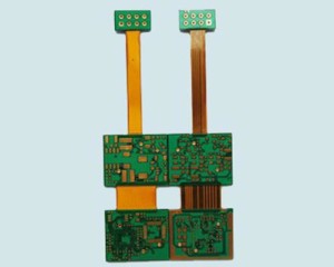
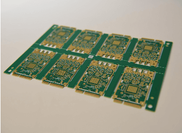
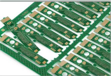
Panelization is commonly performed in PCB production to increase the efficiency of SMT production lines.PCBs typically come in “multi-in-one”configurations,such as 2-in-1 and 4-in-1.
If you’ve had the opportunity to walk through an SMT production line, you’ll find that the biggest bottleneck is the size of the PCB,the printing time is generally around 25 seconds.This means that is the more expensive high-speed SMT printer and general-purpose printer,the printing process is in vain.From an economic perspective,this is a waste of time.
In reality,placement machines are incredibly fast,capable of placing multiple components per second.Some even have multiple nozzles capable of placing components simultaneously.Considering the number of component on a current mobile phone PCBA,a single board should require less than 10 seconds to complete all placement operations.Therefore,by panelizing the PCB to increase the number of component that can be placed,placement machines can be utilized more efficiently.Of course,it best to balance the production line so that each piece of equipment fully utilized.
Paneling offer another benefit:it saves time when placing and unloading PCBAs,as multiple board can be placed and loaded simultaneously.Subsequent board level testing,if continuous board testing can be performed,can significantly reduce the time wasted in jigs and fixtures.
Finally,some boards may have irregular shapes during design,If panelization can be implemented,waste can be significantly reduced,This is the concept of increasing pcb board utilization.
Disadvantages and limitations of PCB Panelization
While PCB panelization offers many advantages,it still requires cutting into individual board after all PCBA assembly is complete.This adds an extra process step,increases labor time,and increases the risk of collisions during transportation.
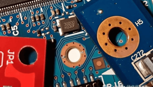
For boards with thin pins or small components like 0201,the number of panels cannot be too large.This is because individual board have tolerances,If too many panels are assembled,the tolerances.If too many panels are assembled ,the tolerance may be too large to meet the required solder paste printing accuracy,resulting in uneven solder paste printing and soldering problems.
For thin PCBs,excessive panelization is also not recommended.The thinner the PCB,the greater the deformation.Excessive panelization increases the width,making SMT placement and reflow oven processing more challenging.Of course,this can be overcome using oven carries or full-process carriers,but the costs must be considered.
What is the purpose of PCB edge fabrication?
PCB edges,also known as coupons abroad,are similar to coupons at convenience stores and can be broken off.However,for quality resons,we do not recommend manually breaking off excess board edges,Instead,machines should be used to remove the edges to reduce the stress caused by the broken edges on the board and components
PCB edge design primarily assists in assembly production.Today’s SMT production lines are highly automated,and boards are transported by belts and chains.As you might have guessed,the primary purpose of the board edges is to provide space for these belts and chains to move the boards.
Of course,if desired,you can leave some space around the board to avoid placing any electronic components.Generally,a minimum of 5.0mm is recommended,as the reflow oven chains require a relatively deep board edge.This allows you to avoid designing board edges,as belts and chains could damage surrounding electronic components.
PCB edges also have other uses:
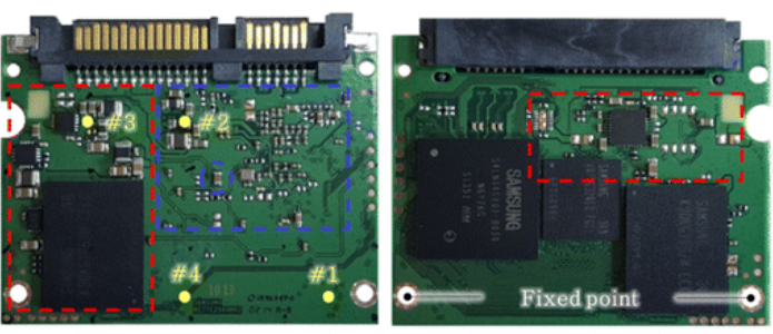
They can be used to position fixture holes for post-SMT ICT or FVT testing to prevent misalignment between the needle bed and the test points.
They can be used to position fixture holes for post-SMT ICT or FVT testing to prevent misalignment between the needle bed and the test points.
They can also be used by SMT production line sensors to detect the position of the circuit boards.Typically,each machine on an SMT production line has a sensor to detect the arrival of a subsequent board,ensuring that only one panel is currently being processed.Otherwise,a new panel might be inserted before the previous one is finished,disrupting the machine and making it unclear which panel to process.Some board may have holes right where the SMT Production line sensors detect them,typically at the top left corner.In these cases,the board edge can be used to create a solid area for the sensors to detect.
For some boards where space constraints prevent the installation of multiple optical positioning points,placement on the board edge is acceptable.However,it is recommended that component trays near narrow pins within the board also have positioning points to increase placement accuracy.