Disadvantages of the traditional four-layer stackup of PCB
If the interlayer capacitance is not large enough, the electric field will be distributed over a relatively large area of the board, so that the interlayer impedance is reduced and the return current can flow back to the top layer. In this case, the field generated by this signal may interfere with the field of the signal of the nearby changed layer. This is not what we want at all. Unfortunately, on a 0.062-inch 4-layer board, the distance between the layers is far (at least 0.020 inches, as shown in Figures 1 and 2), and the interlayer capacitance is small.
The first problem with the stackup in Figures 1 and 2 occurs when the trace changes from layer 1 to layer 4 or vice versa. As shown in Figure 3.
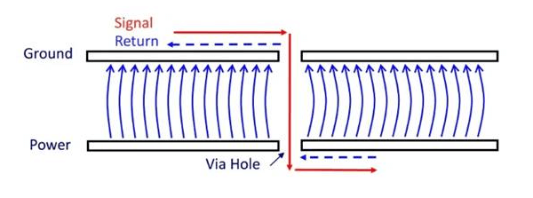
Figure 3. Image provided by Altium.
The figure shows that when the signal trace goes from layer 1 to layer 4 (red line), the return current must also change planes (blue line). If the frequency of the signal is high enough and the planes are close together, the return current can flow through the inter-layer capacitance that exists between the ground and power planes. However, the lack of a direct conductive connection for the return current causes a break in the return path, which we can imagine as impedance between the planes (see Figure 4).
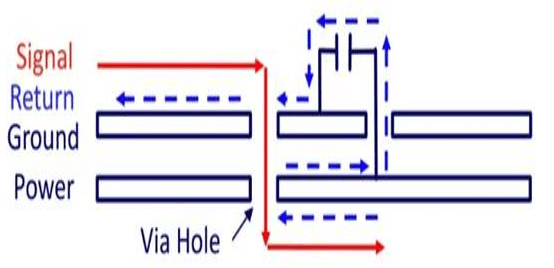
Figure 4. Image courtesy of Electromagnetic Compatibility Engineering.
If the inter-layer capacitance is not large enough, the electric field will be distributed over a relatively large area of the board, so that the inter-layer impedance is reduced and the return current can flow back to the top layer. In this case, the field generated by this signal may interfere with the field of the nearby signal that changed layers. This is not what we want at all. Unfortunately, on a 0.062-inch 4-layer board, the distance between the layers is far (at least 0.020 inches, as shown in Figures 1 and 2), and the inter-layer capacitance is small. Therefore, the above-mentioned electric field interference occurs. This may not cause signal integrity problems, but it will definitely generate more EMI. This is why we avoid changing layers when using the stackup shown in Figures 1 and 2, especially for high-frequency signals such as clocks.
It is common practice to add a decoupling capacitor near the transition via to reduce the impedance experienced by the return current (see Figure 5). However, this decoupling capacitor is ineffective for very high frequency signals due to its low self-resonant frequency. For AC signals above 200-300 MHz, we cannot rely on decoupling capacitors to create a low impedance return path. Therefore, we need a decoupling capacitor (for below 200-300 MHz) and a relatively large inter-board capacitance for higher frequencies.
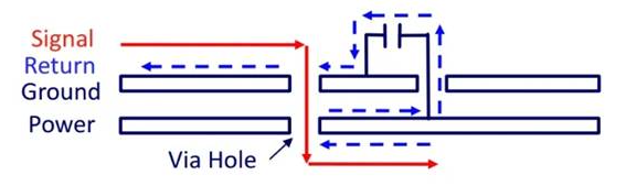
Figure 5 Image provided by Altium.
The above problems can be avoided by not changing the layers of critical signals. However, the small inter-board capacitance of the four-layer board leads to another serious problem: power delivery. Clocking digital ICs usually requires large transient power currents. As the rise/fall time of IC outputs decreases, we need to provide energy at a higher rate. To provide a charge source, we usually place decoupling capacitors very close to each logic IC. However, there is a problem: when we exceed the self-resonant frequency, the decoupling capacitor cannot effectively store and transfer energy because at these frequencies, the capacitor will act like an inductor.
Since most of today’s ICs have fast rise/fall times (about 500 ps), we need an additional decoupling structure with a self-resonant frequency higher than that of the decoupling capacitor. The inter-layer capacitance of the circuit board can be an effective decoupling structure, provided that the layers are close enough to each other to provide sufficient capacitance. Therefore, in addition to the commonly used decoupling capacitors, we prefer to adopt closely spaced power and ground planes to provide transient power to digital ICs.
Note that due to the common circuit board manufacturing process, we usually do not have a thin insulator between the second and third layers of a four-layer board. The cost of a four-layer board with a thin insulator between layers 2 and 3 can be much higher than a traditional four-layer board.


